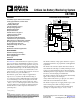
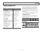
Lithium Ion Battery Monitoring System AD7280A Lithium ion battery monitoring Electric and hybrid electric vehicles Power supply backup Power tools VIN6 VIN5 VIN4 VIN3 VIN2 VIN1 VIN0 AUX6 AUX5 AUX4 AUX3 AUX2 AUX1 HV MUX DAISY-CHAIN INTERFACE CELL BALANCING INTERFACE AD7280A REGULATOR VREG DGND 12-BIT ADC CLOCK CONTROL LOGIC AND SELF-TEST AUXTERM VREF LIMIT REG SQN LOGIC DATA MEMORY SPI INTERFACE 2.
AD7280A TABLE OF CONTENTS Features .............................................................................................. 1 Register Map ................................................................................... 28 Applications ....................................................................................... 1 Cell Voltage Registers ................................................................ 28 Functional Block Diagram .........................................................
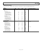
AD7280A SPECIFICATIONS VDD = 8 V to 30 V, VSS = 0 V, DVCC = AVCC = VREG, VDRIVE = 2.7 V to 5.5 V, TA = −40°C to +105°C, unless otherwise noted. Table 1. Parameter DC ACCURACY (VIN0 TO VIN6) 1 Resolution Integral Nonlinearity Differential Nonlinearity Offset Error Offset Error Match Gain Error Gain Error Match ADC Unadjusted Error 2, 3 Total Unadjusted Error 4, 5 Min Typ Reference Voltage Temperature Coefficient Test Conditions/Comments No missing codes ±9 ±10 ±14.
AD7280A Parameter REGULATOR OUTPUT (VREG) Input Voltage Range Output Voltage, VREG 13 Output Current 14 Line Regulation Load Regulation Internal Short Protection Limit CELL BALANCING OUTPUTS 15 Output High Voltage, VOH Output Low Voltage, VOL CB1 Output Ramp-Up Time 16 CB1 Output Ramp-Down Time 17 CB2 to CB6 Output Ramp-Up Time16 CB2 to CB6 Output Ramp-Down Time17 LOGIC INPUTS Input High Voltage, VINH Input Low Voltage, VINL Input Current, IIN Input Capacitance, CIN LOGIC OUTPUTS Output High Voltage, VOH Ou
AD7280A POWER SPECIFICATIONS VDD = 8 V to 30 V, VSS = 0 V, DVCC = AVCC = VREG, VDRIVE = 2.7 V to 5.5 V, TA = −40°C to +105°C, unless otherwise noted. Table 2.
AD7280A TIMING SPECIFICATIONS VDD = 8 V to 30 V, VSS = 0 V, DVCC = AVCC = VREG, VDRIVE = 2.7 V to 5.5 V, TA = −40°C to +105°C, unless otherwise noted. Table 3.
AD7280A ABSOLUTE MAXIMUM RATINGS TA = 25°C, unless otherwise noted. Table 4.
AD7280A AUX2 AUX1 CREF VREF REFGND ALERThi SDIhi CNVSThi SDOhi SCLKhi CShi PDhi PIN CONFIGURATION AND FUNCTION DESCRIPTIONS 48 47 46 45 44 43 42 41 40 39 38 37 VIN6 1 CB6 36 AUX3 PIN 1 2 35 AUX4 VIN5 3 34 AUX5 CB5 4 33 AUX6 VIN4 5 32 AUXTERM AD7280A CB4 6 31 AGND TOP VIEW (Not to Scale) VIN3 7 30 AVCC CB3 8 29 VDRIVE VIN2 9 28 ALERTlo CB2 10 27 ALERT VIN1 11 26 SDO CB1 12 25 SDOlo 09435-003 CNVST SDI SCLK CS DGND DVCC VREG VSS VDD PD VIN0 MASTER 13 14 15
AD7280A Pin No. 21 Mnemonic CS 22 SCLK 23 SDI 24 CNVST 25 SDOlo 26 SDO 27 ALERT 28 ALERTlo 29 VDRIVE 30 AVCC 31 AGND 32 AUXTERM 33 to 38 AUX6 to AUX1 39 40 CREF VREF 41 REFGND 42 ALERThi Description Chip Select Input. The CS input is used to frame the input and output data on the SPI and daisy-chain interfaces. On the master AD7280A device, the CS input is supplied from the DSP/microprocessor.
AD7280A Pin No. 43 Mnemonic SDIhi 44 CNVSThi 45 SDOhi 46 SCLKhi 47 CShi 48 PDhi Description Serial Data Input in Daisy-Chain Mode. The data from each AD7280A in the daisy chain is passed through the SDOlo output and the SDIhi input of each AD7280A in the chain and is supplied to the DSP/microprocessor through the SDO output of the master AD7280A. This input should be connected to the SDOlo output of the AD7280A immediately above it in potential in the daisy chain.
AD7280A TYPICAL PERFORMANCE CHARACTERISTICS 5.5 VDD VDD VDD VDD 7 6 MASTER CURRENTS 5 4 5.1 SLAVE, VDD = 8V SLAVE, VDD = 10V SLAVE, VDD = 29.9V MASTER, VDD = 8V MASTER, VDD = 10V MASTER, VDD = 29.9V 3 2 –20 0 20 40 60 80 100 TEMPERATURE (°C) 1 –40 09435-102 4.9 –40 VDD VDD VDD VDD 5.4 0 20 40 60 80 100 TEMPERATURE (°C) Figure 7. IDD During Cell Balancing vs. Temperature for Different Supply Voltages Figure 4. VREG vs.
AD7280A 10,000 2.506 VREF VOLTAGE (V) 6000 4000 2000 2664 2665 2666 2667 2668 CODE 2.502 2.500 2.496 –40 –20 0 20 7.5 VDD VDD VDD VDD VDD TOTAL UNADJUSTED ERROR (mV) NUMBER OF OCCURRENCES 6.0 8000 6000 4000 2000 692 236 CODE TOTAL UNADJUSTED ERROR (mV) 2.502 2.501 2.500 2.499 2.498 2.497 0 1.5 0 –1.5 –3.0 –20 0 20 20 40 60 80 40 VDD VDD VDD VDD VDD 6.0 2.503 –20 = 8V = 10V = 16.8V = 22.5V = 29.9V 3.0 7.5 = 8V = 10V = 16.8V = 22.5V = 29.9V 2.504 2.
AD7280A 7.5 VDD VDD VDD VDD VDD 4.5 5 4 VOLTAGE (V) 3.0 1.5 0 2 1 0 20 40 60 80 100 0 TEMPERATURE (°C) 4 4 VOLTAGE (V) 5 3 2 4 6 8 10 TIME (ms) 10 8 PD VREG VREF 3 2 0 09435-115 2 6 1 PD VREG VREF 0 4 Figure 19. Power-Up Time, 10 μF Capacitor on the VREF and VREG Pins 5 0 2 TIME (ms) Figure 16. Total Unadjusted Error for Auxiliary Channels (Absolute Value) vs. Temperature for Different Supply Voltages 1 0 Figure 17.
AD7280A TERMINOLOGY Differential Nonlinearity (DNL) DNL is the difference between the measured and the ideal 1 LSB change between any two adjacent codes in the ADC. Integral Nonlinearity (INL) INL is the maximum deviation from a straight line passing through the endpoints of the ADC transfer function. The endpoints of the transfer function are zero scale (a point 1 LSB below the first code transition) and full scale (a point 1 LSB above the last code transition).
AD7280A THEORY OF OPERATION The AD7280A is a lithium ion (Li-Ion) battery monitoring chip that can monitor the voltage and temperature of four, five, or six series-connected Li-Ion battery cells. The AD7280A also provides an interface that can be used to control external transistors for cell balancing. The VDD and VSS supplies required by the AD7280A should be taken from battery cells being monitored by the part.
AD7280A ANALOG INPUT STRUCTURE VIN6 VIN5 VIN4 VIN3 VIN2 VIN0 ADC V IN– 09435-005 ADC V IN+ VDD Figure 23. Mux Configuration During VIN2 to VIN1 Sampling The ADC is a successive approximation register analog-todigital converter (SAR ADC). The converter is composed of a comparator, a SAR, control logic, and two capacitive DACs. Figure 24 shows a simplified schematic of the converter. During the acquisition phase, the SW1, SW2, and SW3 switches are closed.
AD7280A TYPICAL CONNECTION DIAGRAMS 10kΩ 10kΩ 10kΩ 10kΩ 10kΩ 10kΩ 10kΩ 10kΩ 10kΩ 10kΩ 10kΩ 10kΩ 10kΩ 10µF VIN6 10kΩ VDD MASTER VREG CB6 DVCC VIN5 AVCC CB5 VDRIVE VIN4 VREF CB4 AD7280A CREF VIN3 0.1µF 0.1µF 1µF 0.1µF OPTIONAL INTERFACE PINS CB3 ALERT VIN2 CNVST PD CB2 SDO VIN1 DSP/MICROPROCESSOR SCLK SDI CB1 VIN0 1µF VSS CS 4-WIRE SPI INTERFACE 09435-010 0.1µF Figure 28.
AD7280A 1kΩ VDDn 10kΩ 100nF 10kΩ 100nF 10kΩ 100nF 10kΩ 100nF SDIhi CShi VIN5 ALERThi 100nF SDOhi 10kΩ CNVSThi 100nF SCLKhi 10kΩ VIN6 PDhi 10kΩ VREG DVCC AVCC 1µF 0.1µF VDRIVE VIN4 ALERT AD7280A VIN3 SDO VIN2 MASTER VIN1 1kΩ 1kΩ 10kΩ ALERTlo SDOlo SDI SCLK PD CNVST 1µF VIN0 CS VDD(n – 1) VSS 100nF VDDn 100nF VDD 10µF VREF CREF 0.
AD7280A The conversion sequence—that is, the order in which the cell voltages and auxiliary ADC inputs are converted—is shown in Figure 31 and Figure 32. The cell voltage inputs are converted in reverse order, that is, Cell 6 is followed by Cell 5, and so on. However, the auxiliary ADC inputs are converted in increasing numerical order, that is, AUX1 is followed by AUX2, and so on.
AD7280A Note that 90 μs should be allowed before initiating any conversions following any change to Bits[D15:D14]. This time should be allowed between writing to the control register to change the selected conversions and initiating the first conversion. Conversions that are initiated by the rising edge of the CS pin require two separate write commands to the control register.
AD7280A device in the chain can be determined by multiplying tDELAY by the number of slave AD7280As in the daisy chain. The total conversion time for all cell voltage and auxiliary ADC input conversions can be calculated using the following equation: The 10 kΩ resistors in series with the inputs provide protection for the analog inputs in the event of an overvoltage or undervoltage on those inputs.
AD7280A CONVERSION WINDOW CONNECTION OF FEWER THAN SIX VOLTAGE CELLS As described in the Converting Cell Voltages and Auxiliary ADC Inputs section, the AD7280A converts the selected cell voltage and auxiliary ADC inputs in a defined sequence (see Figure 31). As described in the Circuit Information section, the AD7280A consists primarily of a high voltage input multiplexer, a low voltage input multiplexer, and a SAR ADC.
AD7280A AUXILIARY ADC INPUTS AD7280A VSS The AD7280A provides six single-ended analog inputs to the ADC—AUX1 to AUX6—which can be used to convert the voltage output of a thermistor temperature measurement circuit. In the event that no temperature measurements are required or that individual cell temperature measurements are not required, the auxiliary ADC inputs can be used to convert any other 0 V to 5 V input signal.
AD7280A VDD 0.1µF The AD7280A provides two power-down options. Full power-down (hardware) Software power-down 10kΩ VDD MASTER VREG 1µF DVCC Full Power-Down (Hardware) The AD7280A can be placed into full power-down mode, which requires only 5 μA maximum current, by taking the PD pin low. The falling edge of the PD pin powers down all analog and digital circuitry.
AD7280A Software Power-Down CELL BALANCING OUTPUTS The AD7280A can be placed into software power-down mode, which requires 3.8 mA of current, by setting Bit D8 in the control register through the serial interface. The CNVST pin should be gated out before generating a software power-down (see the CNVST Control Register section).
AD7280A An example of how damage to the external transistors can occur is a connection sequence that first provides the system ground (the ground supply to the master AD7280A in the daisy chain) followed by a connection from any of the battery cells at a potential high enough to exceed the VGS of the cell balancing transistor, for example 40 V.
AD7280A ALERT OUTPUT Table 12. Alert Register Settings, Bits[D3:D0]1 The alert output on the AD7280A can be used to indicate whether any of the following faults has occurred: Bits[D3:D2] 00 Bits[D1:D0] XX 01 XX 10 XX 11 XX XX 00 XX 01 XX 10 XX 11 • • • • Cell overvoltage Cell undervoltage Auxiliary ADC overvoltage Auxiliary ADC undervoltage Following each completed conversion, the cell voltage and auxiliary ADC measurement results are compared to the alert thresholds.
AD7280A REGISTER MAP Table 13. Register Name Cell Voltage 1 Cell Voltage 2 Cell Voltage 3 Cell Voltage 4 Cell Voltage 5 Cell Voltage 6 AUX ADC 1 AUX ADC 2 AUX ADC 3 AUX ADC 4 AUX ADC 5 AUX ADC 6 Self-Test Control Cell Overvoltage Cell Undervoltage AUX ADC Overvoltage AUX ADC Undervoltage Alert Cell Balance CB1 Timer CB2 Timer CB3 Timer CB4 Timer CB5 Timer CB6 Timer PD Timer Read CNVST Control Table 14.
AD7280A Select Conversion Inputs Thermistor Termination Resistor Bits[D15:D14] of the control register determine which cell voltages and auxiliary ADC inputs are converted following a convert start command. The default value of D15 and D14 on power-up is 00. Bit D3 of the control register should be set if the user wishes to use a single thermistor termination resistor on the AUXTERM pin.
AD7280A CELL UNDERVOLTAGE REGISTER CELL BALANCE REGISTER The cell undervoltage register determines the low voltage threshold of the AD7280A. Cell voltage conversions lower than the undervoltage threshold trigger the alert output. The AD7280A allows the user to set the undervoltage threshold to a value from 1 V to 5 V. The resolution of the undervoltage threshold is eight bits, that is, 16 mV. The default value of the undervoltage threshold on power-up is 0x00 (1 V).
AD7280A PD TIMER REGISTER CNVST CONTROL REGISTER The PD timer register allows the user to configure a set time after which the AD7280A is automatically powered down. The AD7280A allows the user to set the PD timer to a value from 0 minutes to 36.9 minutes. The resolution of the PD timer is 71.5 sec. When using the PD timer in conjunction with the CBx timers, the value programmed to the PD timer should exceed that programmed to the CBx timer by at least 71.
AD7280A SERIAL INTERFACE The AD7280A serial interface is Mode 1 SPI compliant, that is, the clock polarity (CPOL) is 0, and the clock phase (CPHA) is 1. The interface consists of four signals: CS, SCLK, SDI, and SDO. The SDI line is used to transfer data into the on-chip registers, and the SDO line is used to read the on-chip registers and conversion result registers. SCLK is the serial clock input for the device; all data transfers, either on SDI or on SDO, take place with respect to SCLK.
AD7280A READING FROM THE AD7280A Register Address There are two types of read operation for the AD7280A: The register map for the AD7280A is provided in Table 13. Each register address is six bits long and is used when writing to or reading from the on-chip registers of the AD7280A.
AD7280A DAISY-CHAIN INTERFACE In a battery monitoring application, up to eight AD7280As can be daisy-chained together to allow up to 48 individual lithium ion cell voltages to be monitored. Each AD7280A is capable of monitoring up to six Li-Ion cells and is powered from the top and bottom voltage of the six Li-Ion cells. As a result, the supply voltages of each AD7280A are offset by up to 30 V from adjacent AD7280As in the chain.
AD7280A For example, to read back the write acknowledge bit from Device 1 in the chain after writing to a register on that device, the read operation of Device 0, the master device, must be turned off. Also, the SCLK frequency must be lower than 1 MHz when reading back the write acknowledge bit from devices higher in the chain than the master device in this mode.
AD7280A Read Operation CRC CRC Calculation Example 1 For reads from the AD7280A, the 8-bit CRC is generated by the AD7280A based on Bits[D31:D10] of the 32-bit read cycle and is transmitted using Bits[D9:D2] of the same read cycle. The data received is divided by the CRC polynomial, and the 8-bit remainder, following the division, becomes the CRC bits, CRC_7 to CRC_0.
AD7280A CRC Calculation Example 3 CRC Calculation Example 4 This example shows the breakdown of a 32-bit register read from the low byte of the control register of the master device, that is, Device 0. This example shows the breakdown of a 32-bit conversion result read from the Cell Voltage 3 conversion result register of Device 1.
AD7280A EXAMPLES OF INTERFACING WITH THE AD7280A The AD7280A supports a number of read options. The user can read back the results from • • • All conversions completed on all parts in the chain Individual registers on all parts in the chain Individual registers on selected parts in the chain In each case, the user must first write to the read register on the selected parts to configure that part to supply the correct data on the outputs.
AD7280A Example 1: Initialize All Parts in a Daisy Chain on Initial Power-Up and When Coming Out of Power-Down Example 2: Convert and Read All Parts, All Voltages, and All Auxiliary ADC Inputs Example 1 shows a typical device initialization routine. In this example, it is assumed that all AD7280As in the daisy chain have been initialized to their correct device addresses. 1. 2. 3.
AD7280A Example 3: Convert and Read All Parts, All Voltages, and Three Auxiliary ADC Inputs per Part Program the CNVST control register to 0x02 on all parts to allow conversions to be initiated using the CNVST pin. The 32-bit write command is 0x03A0546A (see Table 25, Write 3). Initiate conversions through the falling edge of CNVST. Allow sufficient time for all conversions to be completed plus tWAIT.
AD7280A Example 4: Convert and Read a Single Voltage or Auxiliary ADC Input Result from One Part Program the CNVST control register to 0x02 on Device 3 to allow conversions to be initiated using the CNVST pin on that part. The 32-bit write command is 0xC3A0417A (see Table 26, Write 4). Initiate conversions through the falling edge of CNVST. Allow sufficient time for all conversions to be completed plus tWAIT. Program the CNVST control register to gate the CNVST signal on all parts.
AD7280A Example 5: Read a Single Configuration Register on All Parts Example 6: Read a Single Configuration Register from One Part In this example, it is assumed that all AD7280As in the daisy chain have been initialized to their correct device addresses. In this example, it is assumed that all AD7280As in the daisy chain have been initialized to their correct device addresses. 1. 1. 2. 3. Set Bit D0 of the control register to 1 on all parts.
AD7280A Example 7: Self-Test Conversion on All Parts The CNVST control register should be programmed to gate the CNVST signal on all parts. The 32-bit write command is 0x03A0340A (see Table 29, Write 5). This write prevents unintentional conversions from being initiated by noise or glitches on the CNVST pin. This write also updates the on-chip output registers of all devices in the daisy chain. Apply a CS low pulse that frames 32 SCLKs to read back the desired voltage.
AD7280A EMC GUIDELINES Note that these ferrite beads can be replaced with a small value of resistance. The maximum value of resistance that can be used is 20 Ω. A resistor should not be included on the VSS line to the master chip. Instead, a direct connection should be made from the battery cell connector to the VSS pin.
AD7280A to gate the convert start signal. This prevents any glitches that occur on the CNVST pin from being applied directly to the internal circuitry of the AD7280A. If a second convert start signal is received by the AD7280A while the conversion results are being read back, the data being read back from the device, or chain of devices, can be corrupted. The corruption of data occurs at the point in which the second convert start signal is introduced.
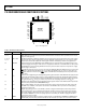
AD7280A OUTLINE DIMENSIONS 9.20 9.00 SQ 8.80 1.60 MAX 37 48 36 1 PIN 1 7.20 7.00 SQ 6.80 TOP VIEW 1.45 1.40 1.35 0.15 0.05 0.20 0.09 7° 3.5° 0° 0.08 COPLANARITY SEATING PLANE VIEW A (PINS DOWN) 25 12 13 VIEW A 0.50 BSC LEAD PITCH ROTATED 90° CCW COMPLIANT TO JEDEC STANDARDS MS-026-BBC 24 0.27 0.22 0.17 051706-A 0.75 0.60 0.45 Figure 42.
AD7280A NOTES Rev.
AD7280A NOTES ©2011 Analog Devices, Inc. All rights reserved. Trademarks and registered trademarks are the property of their respective owners. D09435-0-4/11(0) Rev.