
Datasheet


AD7280A
Rev. 0 | Page 3 of 48
SPECIFICATIONS
V
DD
= 8 V to 30 V, V
SS
= 0 V, DV
CC
= AV
CC
= V
REG
, V
DRIVE
= 2.7 V to 5.5 V, T
A
= −40°C to +105°C, unless otherwise noted.
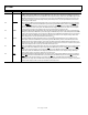
Table 1.
Parameter Min Typ Max Unit Test Conditions/Comments
DC ACCURACY (VIN0 TO VIN6)
1
Resolution 12 Bits No missing codes
Integral Nonlinearity ±1 LSB
Differential Nonlinearity ±0.8 LSB
Offset Error ±1 LSB
Offset Error Match 1 LSB
Gain Error ±1 LSB
Gain Error Match 1 LSB
ADC Unadjusted Error
2, 3
±1.2 mV
Total Unadjusted Error
4, 5
±9 mV V
IN
range
6
= 1 V to 4.1 V, −10°C to +85°C
±10 mV V
IN
range
6
= 1 V to 4.1 V, −40°C to +85°C
±1.6 ±14.5 mV V
IN
range
6
= 1 V to 4.1 V, −40°C to +105°C
CELL VOLTAGE INPUTS (VIN0 TO VIN6)
Pseudo Differential Input Voltage
VIN(x) − VIN(x − 1) 1 2 × V
REF
V
Absolute Input Voltage V
CM
− V
REF
V
CM
+ V
REF
V
Common-Mode Input Voltage 0.5 27.5 V
Static Leakage Current
7
±5 ±70 nA
Dynamic Leakage Current
7
±3 nA
CNVST
pulse every 100 ms
Input Capacitance 15 pF
DC ACCURACY (AUX1 TO AUX6)
1, 8
Resolution 12 Bits No missing codes
Integral Nonlinearity ±1 LSB
Differential Nonlinearity ±0.8 LSB
Offset Error ±2 LSB
Offset Error Match 2 LSB
Gain Error ±2 LSB
Gain Error Match 2 LSB
ADC Unadjusted Error
9
±1.2 mV
Total Unadjusted Error
10
±20 mV −40°C to +85°C
±1.6 ±22 mV −40°C to +105°C
AUXILIARY ADC INPUTS (AUX1 TO AUX6)
Input Voltage Range 0 2 × V
REF
V
Static Leakage Current
7
±15 nA
Dynamic Leakage Current
7
±3 nA
CNVST
pulse every 100 ms
Input Capacitance 15 pF
REFERENCE
Reference Voltage 2.494 2.5 2.506 V −40°C to +85°C
2.494 2.5 2.509 V −40°C to +105°C
Reference Voltage Temperature
Coefficient
±3 ±15 ppm/°C −40°C to +85°C
±11 ppm/°C −40°C to +105°C
Output Voltage Hysteresis 50 ppm −40°C to +105°C
Long-Term Drift 150
ppm/1000
hours
Line Regulation ±5 ppm/V
Turn-On Settling Time
11, 12
5.5 10 ms V
REG
= 1 µF, V
REF
= 1 µF, C
REF
= 100 nF