
Datasheet


AD7280A
Rev. 0 | Page 6 of 48
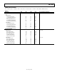
TIMING SPECIFICATIONS
V
DD
= 8 V to 30 V, V
SS
= 0 V, DV
CC
= AV
CC
= V
REG
, V
DRIVE
= 2.7 V to 5.5 V, T
A
= −40°C to +105°C, unless otherwise noted.
Table 3.
Parameter
1
Min Typ Max Unit Description
t
CONV
ADC conversion time
425 560 695 ns −40°C to +85°C
425 720 ns −40°C to +105°C
t
ACQ
ADC acquisition time, Bits[D6:D5] of the control register set to 00
340 400 465 ns −40°C to +85°C
340 470 ns −40°C to +105°C
t
ACQ
ADC acquisition time, Bits[D6:D5] of the control register set to 01
665 800 1010 ns −40°C to +85°C
665 1030 ns −40°C to +105°C
t
ACQ
ADC acquisition time, Bits[D6:D5] of the control register set to 10
1005 1200 1460 ns −40°C to +85°C
1005 1510 ns −40°C to +105°C
t
ACQ
ADC acquisition time, Bits[D6:D5] of the control register set to 11
1340 1600 1890 ns −40°C to +85°C
1340 1945 ns −40°C to +105°C
t
DELAY
200 250 ns
Propagation delay between the falling edges of CNVST
of adjacent
parts in the daisy chain
t
WAIT
5 s
Time required between the end of conversions and the beginning
of readback of the conversion results
f
SCLK
1 MHz Frequency of serial read clock
t
QUIET
200 ns
Minimum quiet time required between the end of a serial read and
the start of the next conversion
t
1
2
0.4 50 µs
CNVST
low pulse
t
2
10 ns
CS
falling edge to SCLK rising edge
t
3
20 ns
Delay from CS
falling edge until SDO is three-state disabled
t
4
5 ns SDI setup time prior to SCLK falling edge
t
5
4 ns SDI hold time after SCLK falling edge
t
6
3
28 ns Data access time after SCLK rising edge
t
7
20 ns SCLK to data valid hold time
t
8
0.45 × t
SCLK
ns SCLK high pulse width
t
9
0.45 × t
SCLK
ns SCLK low pulse width
t
10
4
100 ns
CS
rising edge to SCLK rising edge
t
11
10 ns
CS
rising edge to SDO high impedance
t
12
3 µs
CS
high time required between each 32-bit write/read command
1
Sample tested during initial release to ensure compliance. All input signals are specified with t
R
= t
F
= 5 ns (10% to 90% of V
DRIVE
) and timed from a voltage level of 1.6 V.
All timing specifications given are with a 25 pF load capacitance.
2
Maximum allowed
CNVST
low pulse time to ensure that a software power-down state is not entered when the
CNVST
pin is not gated.
3
Time required for the output to cross 0.4 V or 2.4 V.
4
t
10
applies when using a continuous SCLK. Guaranteed by design.
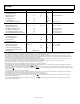
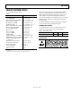
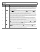
Timing Diagram
0
9435-020
t
8
t
10
THREE-STATETHREE-STATE
S
CLK
SDO
SDI
LSBMSB MSB – 1
MSB MSB – 1
324321
LSB
t
12
t
2
3
t
6
t
t
7
t
4
t
5
t
11
t
9
CS
Figure 2. Serial Interface Timing Diagram