
Datasheet


AD7280A
Rev. 0 | Page 8 of 48
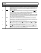
PIN CONFIGURATION AND FUNCTION DESCRIPTIONS
48
PDhi
47
CShi
46
SCLKhi
45
SDOhi
44
CNVSThi
43
SDIhi
42
ALERThi
41
REFGND
40
V
REF
39
C
REF
38
AUX1
37
AUX2
35
AUX4
34
AUX5
33
AUX6
30
AV
CC
31
AGND
32
AUX
TERM
36
AUX3
29
V
DRIVE
28
ALERTlo
27
ALERT
25
SDOlo
26
SDO
2
CB6
3
V
IN5
4
CB5
7
V
IN3
6
CB4
5
V
IN4
1
V
IN6
8
CB3
9
V
IN2
10
CB2
12
CB1
11
V
IN1
13
VIN0
14
MASTER
15
PD
16
V
DD
17
V
SS
18
V
REG
19
DV
CC
20
DGND
21
CS
22
SCLK
23
SDI
24
CNVST
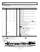
PIN 1
AD7280A
TOP VIEW
(Not to Scale)
09435-003
Figure 3. Pin Configuration
Table 6. Pin Function Descriptions
Pin No. Mnemonic Description
1, 3, 5, 7, 9,
11, 13
VIN6 to VIN0
Analog Input 6 to Analog Input 0. VIN0 should be connected to the base of the series-connected battery cells.
VIN1 should be connected to the top of Cell 1, VIN2 should be connected to the top of Cell 2, and so on (see
Figure 28 and Figure 29).
2, 4, 6, 8,
10, 12
CB6 to CB1
Cell Balance Output 6 to Cell Balance Output 1. These pins provide a voltage output that can be used to supply
the gate drive of an external cell balancing transistor. Each CBx output provides a 0 V or 5 V voltage output
referenced to the absolute amplitude of the negative terminal of the battery cell that is being balanced.
14 MASTER
Voltage Input. Connect the MASTER pin of the AD7280A that is connected directly to the DSP/microprocessor
to the V
DD
supply pin through a 10 kΩ resistor. In an application with two or more AD7280As in a daisy chain,
the MASTER pins of the remaining AD7280As in the daisy chain should be tied to their respective V
SS
supply
pins through 10 kΩ resistors.
15
PD
Power-Down Input. This input is used to power down the AD7280A. When the AD7280A acts as a master, the
PD
input is supplied from the DSP/microprocessor. When the AD7280A acts as a slave in a daisy chain, the
PD
input should be connected to the PDhi output of the AD7280A immediately below it in potential in the
daisy chain.
16 V
DD
Positive Power Supply Voltage for the High Voltage Analog Input Structure of the AD7280A. The supply must be
greater than the minimum voltage of 8 V. V
DD
can be supplied directly from the cell with the highest potential
of the four, five, or six cell battery stacks that the AD7280A is monitoring. The maximum voltage that should
be applied between V
DD
and V
SS
is 30 V. Place 10 µF and 100 nF decoupling capacitors on the V
DD
pin.
17 V
SS
Negative Power Supply Voltage for the High Voltage Analog Input Structure of the AD7280A. This input should
be at the same potential as the AGND/DGND voltage.
18 V
REG
Analog Voltage Output, 5.2 V. The internally generated V
REG
voltage, which provides the supply voltage for
the ADC core, is available on this pin for use external to the AD7280A. Place 1 µF and 100 nF decoupling
capacitors on the V
REG
pin.
19 DV
CC
Digital Supply Voltage, 4.9 V to 5.5 V. The DV
CC
and AV
CC
voltages should ideally be at the same potential.
For best performance, it is recommended that the DV
CC
and AV
CC
pins be shorted together to ensure that
the voltage difference between them never exceeds 0.3 V, even on a transient basis. This supply should be
decoupled to DGND. Place 100 nF decoupling capacitors on the DV
CC
pin. The DV
CC
supply pin should be
connected to the V
REG
output.
20 DGND
Digital Ground. Ground reference point for all digital circuitry on the AD7280A. The DGND and AGND voltages
should ideally be at the same potential and must not be more than 0.3 V apart, even on a transient basis.