
Datasheet

AD736
REV. C
–3–
AD736J/A AD736K/B
Model Conditions Min Typ Max Min Typ Max Units
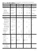
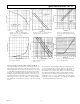
±3 dB Bandwidth Sine-Wave Input
V
IN
= 1 mV rms 5 5 kHz
V
IN
= 10 mV rms 55 55 kHz
V
IN
= 100 mV rms 170 170 kHz
V
IN
= 200 mV rms 190 190 kHz
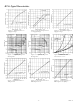
FREQUENCY RESPONSE
Low Impedance Input (Pin 1)
For 1% Additional Error Sine-Wave Input
V
IN
= 1 mV rms 1 1 kHz
V
IN
= 10 mV rms 6 6 kHz
V
IN
= 100 mV rms 90 90 kHz
V
IN
= 200 mV rms 90 90 kHz
±3 dB Bandwidth Sine-Wave Input
V
IN
= l mV rms 5 5 kHz
V
IN
= 10 mV rms 55 55 kHz
V
IN
= 100 mV rms 350 350 kHz
V
IN
= 200 mV rms 460 460 kHz
POWER SUPPLY
OperatingVoltageRange +2.8, –3.2 ±5 ±16.5 +2.8, –3.2 ±5 ±16.5 Volts
Quiescent Current Zero Signal 160 200 160 200 µA
200 mV rms, No Load Sine-Wave Input 230 270 230 270 µA
TEMPERATURE RANGE
Operating, Rated Performance
Commercial (0°C to +70°C) AD736J AD736K
Industrial (–40°C to +85°C) AD736A AD736B
NOTES
l
Accuracy is specified with the AD736 connected as shown in Figure 16 with capacitor C
C
.
2
Nonlinearity is defined as the maximum deviation (in percent error) from a straight line connecting the readings at 0 and 200 mV rms. Output offset voltage is adjusted to zero.
3
Error vs. Crest Factor is specified as additional error for a 200 mV rms signal. C.F. = V
PEAK
/V rms.
4
DC offset does not limit ac resolution.
Specifications are subject to change without notice.
Specifications shown in boldface are tested on all production units at final electrical test.
Results from those tests are used to calculate outgoing quality levels.
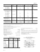
ABSOLUTE MAXIMUM RATINGS
1
Supply Voltage . . . . . . . . . . . . . . . . . . . . . . . . . . . . . . . ±16.5 V
Internal Power Dissipation
2
. . . . . . . . . . . . . . . . . . . . .200 mW
Input Voltage . . . . . . . . . . . . . . . . . . . . . . . ±V
S
Output Short-Circuit Duration . . . . . . . . . . . . . . . . . Indefinite
Differential Input Voltage . . . . . . . . . . . . . . . . . . +V
S
and –V
S
Storage Temperature Range (Q) . . . . . . –65°C to +150°C
Storage Temperature Range (N, R) . . . . . –65°C to +125°C
Operating Temperature Range
AD736J/K . . . . . . . . . . . . . . . . . . . . . . . . . . . 0°C to +70°C
AD736A/B . . . . . . . . . . . . . . . . . . . . . . . . . .–40°C to +85°C
ORDERING GUIDE
Temperature Package Package
Model Range Description Option
AD736JN 0°C to +70°C Plastic Mini-DIP N-8
AD736KN 0°C to +70°C Plastic Mini-DIP N-8
AD736JR 0°C to +70°C Plastic SOIC SO-8
AD736KR 0°C to +70°C Plastic SOIC SO-8
AD736AQ –40°C to +85°C Cerdip Q-8
AD736BQ –40°C to +85°C Cerdip Q-8
AD736JR-REEL 0°C to +70°C Plastic SOIC SO-8
AD736JR-REEL-7 0°C to +70°C Plastic SOIC SO-8
AD736KR-REEL 0°C to +70°C Plastic SOIC SO-8
AD736KR-REEL-7 0°C to +70°C Plastic SOIC SO-8
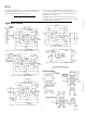
PIN CONFIGURATION
8-Pin Mini-DIP (N-8), 8-Pin SOIC (R-8),
8-Pin Cerdip (Q-8)
Lead Temperature Range (Soldering 60 sec) . . . . . . . . +300°C
ESD Rating . . . . . . . . . . . . . . . . . . . . . . . . . . . . . . . . . . .500 V
NOTES
1
Stresses above those listed under “Absolute Maximum Ratings” may cause
permanent damage to the device. This is a stress rating only and functional
operation of the device at these or any other conditions above those indicated in the
operational section of this specification is not implied. Exposure to absolute
maximum rating conditions for extended periods may affect device reliability .
2
8-Pin Plastic Package: θ
JA
= 165°C/W
8-Pin Cerdip Package: θ
JA
= 110°C/W
8-Pin Small Outline Package: θ
JA
= 155°C/W