
Datasheet

AD736
REV. C
–7–
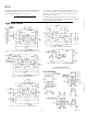
As shown, the dc error is the difference between the average of
the output signal (when all the ripple in the output has been
removed by external filtering) and the ideal dc output. The dc
error component is therefore set solely by the value of averaging
capacitor used-no amount of post filtering (i.e., using a very
large C
F
) will allow the output voltage to equal its ideal value.
The ac error component, an output ripple, may be easily re-
moved by using a large enough post filtering capacitor, C
F
.
In most cases, the combined magnitudes of both the dc and ac
error components need to be considered when selecting appro-
priate values for capacitors C
AV
and C
F
. This combined error,
representing the maximum uncertainty of the measurement is
termed the “averaging error” and is equal to the peak value of
the output ripple plus the dc error.
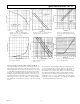
As the input frequency increases, both error components de-
crease rapidly: if the input frequency doubles, the dc error and
ripple reduce to 1/4 and 1/2 their original values, respectively,
and rapidly become insignificant.
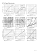
AC MEASUREMENT ACCURACY AND CREST FACTOR
The crest factor of the input waveform is often overlooked when
determining the accuracy of an ac measurement. Crest factor is
defined as the ratio of the peak signal amplitude to the rms am-
plitude (C.F. = V
PEAK
/V rms). Many common waveforms, such
as sine and triangle waves, have relatively low crest factors (≤2).
Other waveforms, such as low duty cycle pulse trains and SCR
waveforms, have high crest factors. These types of waveforms
require a long averaging time constant (to average out the long
time periods between pulses). Figure 6 shows the additional
error vs. crest factor of the AD736 for various values of C
AV
.
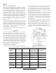
SELECTING PRACTICAL VALUES FOR INPUT
COUPLING (C
C
), AVERAGING (C
AV
) AND FILTERING
(C
F
) CAPACITORS
Table II provides practical values of C
AV
and C
F
for several
common applications.
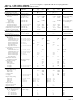
Table II. AD737 Capacitor Selection Chart
Application rms Low Max C
AV
C
F
Settling
Input Frequency Crest Time*
Level Cutoff Factor to 1%
(–3dB)
General Purpose 0–1 V 20 Hz 5 150 µF 10 µF 360 ms
rms Computation 200 Hz 5 15 µF1 µF 36 ms
0–200 mV 20 Hz 5 33 µF 10 µF 360 ms
200 Hz 5 3.3 µF1 µF 36 ms
General Purpose 0–1 V 20 Hz None 33 µF 1.2 sec
Average 200 Hz None 3.3 µF 120 ms
Responding
0–200 mV 20 Hz None 33 µF 1.2 sec
200 Hz None 3.3 µF 120 ms
SCR Waveform 0–200 mV 50 Hz 5 100 µF 33 µF 1.2 sec
Measurement 60 Hz 5 82 µF 27 µF 1.0 sec
0–100 mV 50 Hz 5 50 µF 33 µF 1.2 sec
60 Hz 5 47 µF 27 µF 1.0 sec
Audio
Applications
Speech 0–200 mV 300 Hz 3 1.5 µF 0.5 µF 18 ms
Music 0–100 mV 20 Hz 10 100 µF 68 µF 2.4 sec
*Settling time is specified over the stated rms input level with the input signal increasing
from zero. Settling times will be greater for decreasing amplitude input signals.
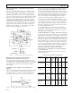
RMS MEASUREMENT – CHOOSING THE OPTIMUM
VALUE FOR C
AV
Since the external averaging capacitor, C
AV
, “holds” the recti-
fied input signal during rms computation, its value directly af-
fects the accuracy of the rms measurement, especially at low
frequencies. Furthermore, because the averaging capacitor ap-
pears across a diode in the rms core, the averaging time constant
will increase exponentially as the input signal is reduced. This
means that as the input level decreases, errors due to nonideal
averaging will reduce while the time it takes for the circuit to
settle to the new rms level will increase. Therefore, lower input
levels allow the circuit to perform better (due to increased aver-
aging) but increase the waiting time between measurements.
Obviously, when selecting C
AV
, a trade-off between computa-
tional accuracy and settling time is required.
Figure 17. AD736 Average Responding Circuit
RAPID SETTLING TIMES VIA THE AVERAGE
RESPONDING CONNECTION (FIGURE 17)
Because the average responding connection does not use the
C
AV
averaging capacitor, its settling time does not vary with in-
put signal level; it is determined solely by the RC time constant
of C
F
and the internal 8 kΩ resistor in the output amplifier’s
feedback path.
DC ERROR, OUTPUT RIPPLE, AND AVERAGING
ERROR
Figure 18 shows the typical output waveform of the AD736 with
a sine-wave input applied. As with all real-world devices, the
ideal output of V
OUT
= V
IN
is never exactly achieved; instead,
the output contains both a dc and an ac error component.
Figure 18. Output Waveform for Sine-Wave Input Voltage