
Datasheet


Data Sheet AD736
Rev. I | Page 5 of 20
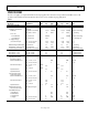
ABSOLUTE MAXIMUM RATINGS
Table 2.
Parameter Rating
Supply Voltage ±16.5 V
Internal Power Dissipation 200 mW
Input Voltage
Pin 2 through Pin 8 ±V
S
Pin 1 ±12 V
Output Short-Circuit Duration Indefinite
Differential Input Voltage
+V
S
and –V
S
Storage Temperature Range (Q) –65°C to +150°C
Storage Temperature Range (N, R) –65°C to +125°C
Lead Temperature (Soldering, 60 sec) 300°C
ESD Rating 500 V
Stresses above those listed under Absolute Maximum Ratings
may cause permanent damage to the device. This is a stress
rating only; functional operation of the device at these or any
other conditions above those indicated in the operational
section of this specification is not implied. Exposure to absolute
maximum rating conditions for extended periods may affect
device reliability.
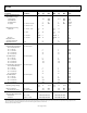
THERMAL RESISTANCE
θ
JA
is specified for the worst-case conditions, that is, a device
soldered in a circuit board for surface-mount packages.
Table 3. Thermal Resistance
Package Type θ
JA
Unit
8-Lead PDIP 165 °C/W
8-Lead CERDIP
110
°C/W
8-Lead SOIC 155 °C/W
ESD CAUTION