
Datasheet


AD7490 Data Sheet
Rev. D | Page 4 of 28
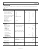
Parameter Test Conditions/Comments Min Typ Max Unit
LOGIC INPUTS
Input High Voltage, V
INH
0.7 × V
DRIVE
V
Input Low Voltage, V
INL
0.3 × V
DRIVE
V
Input Current, I
IN
V
IN
= 0 V or V
DRIVE
±0.01 ±1 µA
Input Capacitance, C
IN
+
3
10
pF
LOGIC OUTPUTS
Output High Voltage, V
OH
I
SOURCE
= 200 µA; V
DD
= 2.7 V to 5.25 V V
DRIVE
− 0.2 V
Output Low Voltage, V
OL
I
SINK
= 200 µA
0.4
V
Floating State Leakage Current
WEAK/
TRI bit set to 0
±10 µA
Floating State Output Capacitance
3
WEAK/
TRI bit set to 0
10 pF
Output Coding Coding bit set to 1 Straight (Natural) Binary
Coding bit set to 0 Twos Complement
CONVERSION RATE
Conversion Time 16 SCLK cycles, SCLK = 20 MHz 800 ns
Track-and-Hold Acquisition Time
2
Sine wave input 300 ns
Full-scale step input 300 ns
Throughput Rate
V
DD
= 5 V (see the Serial Interface
section)
1 MSPS
POWER REQUIREMENTS
V
DD
2.7 5.25 V
V
DRIVE
2.7 5.25 V
I
DD
4
Digital inputs = 0 V or V
DRIVE
Normal Mode (Static) V
DD
= 2.7 V to 5.25 V, SCLK on or off 600 µA
Normal Mode (Operational) V
DD
= 4.75 V to 5.25 V, f
SCLK
= 20 MHz 2.5 mA
(f
S
= Maximum Throughput)
V
DD
= 2.7 V to 3.6 V, f
SCLK
= 20 MHz
1.8
mA
Auto Standby Mode f
SAMPLE
= 500 kSPS 1.55 mA
Static 100 µA
Auto Shutdown Mode f
SAMPLE
= 250 kSPS 960 µA
Static 0.5 µA
Full Shutdown Mode SCLK on or off 0.02 0.5 µA
Power Dissipation
4
Normal Mode (Operational) V
DD
= 5 V, f
SCLK
= 20 MHz 12.5 mW
V
DD
= 3 V, f
SCLK
= 20 MHz 5.4 mW
Auto Standby Mode (Static) V
DD
= 5 V 460 µW
V
DD
= 3 V 276 µW
Auto Shutdown Mode (Static)
V
DD
= 5 V
2.5
µW
V
DD
= 3 V 1.5 µW
Full Shutdown Mode V
DD
= 5 V 2.5 µW
V
DD
= 3 V 1.5 µW
1
Specifications apply for f
SCLK
up to 20 MHz. However, for serial interfacing requirements, see the Timing Specifications section.
2
See the Terminology section.
3
Guaranteed by characterization.
4
See the Power vs. Throughput Rate section.