
Datasheet


Data Sheet AD7490
Rev. D | Page 5 of 28
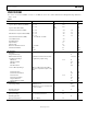
TIMING SPECIFICATIONS
V
DD
= 2.7 V to 5.25 V, V
DRIVE
≤ V
DD
, REF
IN
= 2.5 V; T
A
= T
MIN
to T
MAX
, unless otherwise noted.
Table 2. Timing Specifications
1
Limit at T
MIN
, T
MAX
Parameter V
DD
= 3 V V
DD
= 5 V Unit Description
f
SCLK
2
10 10 kHz min
16 20 MHz max
t
CONVERT
16 × t
SCLK
16 × t
SCLK
t
QUIET
50 50 ns min Minimum quiet time required between bus relinquish and start of next conversion
t
2
12 10 ns min
CS to SCLK setup time
t
3
3
20 14 ns max
Delay from
CS until DOUT three-state disabled
t
3
b
4
30
20
ns max
Delay from CS to DOUT valid
t
4
3
60 40 ns max Data access time after SCLK falling edge
t
5
0.4 × t
SCLK
0.4 × t
SCLK
ns min SCLK low pulse width
t
6
0.4 × t
SCLK
0.4 × t
SCLK
ns min SCLK high pulse width
t
7
15 15 ns min SCLK to DOUT valid hold time
t
8
5
15/50 15/50 ns min/max SCLK falling edge to DOUT high impedance
t
9
20 20 ns min DIN setup time prior to SCLK falling edge
t
10
5 5 ns min DIN hold time after SCLK falling edge
t
11
20 20 ns min
16
th
SCLK falling edge to CS high
t
12
1 1 µs max Power-up time from full power-down/auto shutdown/auto standby modes
1
Guaranteed by characterization. All input signals are specified with t
R
= t
F
= 5 ns (10% to 90% of V
DD
) and timed from a voltage level of 1.6 V (see Figure 2). The 3 V
operating range spans from 2.7 V to 3.6 V. The 5 V operating range spans from 4.75 V to 5.25 V.
2
The mark/space ratio for the SCLK input is 40/60 to 60/40. The maximum SCLK frequency is 16 MHz with V
DD
= 3 V to give a throughput of 870 kSPS. Care must be
taken when interfacing to account for data access time, t
4
, and the setup time required for the user’s processor. These two times determine the maximum SCLK
frequency with which the user’s system can operate (see the Serial Interface section).
3
Measured with the load circuit of Figure 2 and defined as the time required for the output to cross 0.4 V or 0.7 V
DRIVE
.
4
t
3
b represents a worst-case figure for having ADD3 available on the DOUT line, that is, if the AD7490 goes back into three-state at the end of a conversion and some
other device takes control of the bus between conversions, the user has to wait a maximum time of t
3
b before having ADD3 valid on the DOUT line. If the DOUT line is
weakly driven to ADD3 between conversions, the user typically has to wait 17 ns at 3 V and 12 ns at 5 V after the
CS
falling edge before seeing ADD3 valid on DOUT.
5
t
8
is derived from the measured time taken by the data outputs to change 0.5 V when loaded with the circuit of Figure 2. The measured number is then extrapolated
back to remove the effects of charging or discharging the 25 pF capacitor. This means that the time, t
8
, quoted in the timing characteristics, is the true bus relinquish
time of the part and is independent of the bus loading.
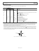
02691-002
200µA I
OL
200µA I
OH
1.6V
T
O OUTPUT
PIN
C
L
25pF
Figure 2. Load Circuit for Digital Output Timing Specifications