
Datasheet


REV. C
–2–
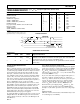
AD75019–SPECIFICATIONS
1
AD75019 Symbol Min Typ Max Units
MULTIPLEXER
Input Signal Range V
IN
V
SS
– 0.5 V
DD
+ 0.5 V
Switch ON Resistance, V
DD
and V
SS
= ±12 V, V
SIGNAL
= ±12 V R
ON
150 300 Ω
Switch ON Resistance, V
DD
and V
SS
= ±5 V, V
SIGNAL
= ±5 V R
ON
300 500 Ω
Switch ON Resistance Matching
2
, V
SIGNAL
= ±12 V ∆R
ON
20 30 Ω
Leakage Current, V
SIGNAL
= ±10 V 2 10 nA
Input/Output Capacitance C
IN
25 pF
Isolation Between Any Two Channels
R
S
= 600 Ω, R
L
= 10 kΩ, V
SIGNAL
= 2 V p-p
f
SIGNAL
= 1 kHz 92 dB
f
SIGNAL
= 20 kHz 69 dB
f
SIGNAL
= 1 MHz 38 dB
Total Harmonic Distortion
R
S
= 600 Ω, R
L
= 10 kΩ, V
SIGNAL
= 2 V p-p 0.01 %
Switch Frequency Response, –3 dB
R
S
= 600 Ω, R
L
= 10 kΩ, V
SIGNAL
= 2 V p-p 20 MHz
Propagation Delay 48 ns
DIGITAL INPUTS (SIN, SCLK, PCLK)
Logic Levels (TTL Compatible)
Input Voltage, Logic “1” V
IH
2.4 5.5 V
Input Voltage, Logic “0” V
IL
0 0.8 V
Input Current, V
IH
= 5.5 V I
IH
±1 µA
Input Current, V
IL
= 0.8 V I
IL
±1 µA
Input Capacitance C
IN
10 pF
DIGITAL OUTPUTS (SOUT)
Logic Levels (TTL Compatible)
Output Voltage, Logic “1” V
OH
2.8 V
Output Voltage, Logic “0” V
OL
0.4 V
Output Current, V
OH
= 2.8 V I
OH
3.2 mA
Output Current, V
OL
= 0.4 V I
OL
3.2 mA
POWER SUPPLY REQUIREMENTS
Voltage Range, Total Analog V
DD
–
V
SS
9.0 25.2 V
Voltage Range, Positive Analog V
DD
– V
DGND
(V
CC
– 0.5) 25.2 V
Voltage Range, Negative Analog V
SS
– V
DGND
–20.7 0 V
Voltage Range, Digital V
CC
– V
DGND
4.5 5 5.5 V
Supply Current, SCLK = 5 MHz, I
DD
, I
SS
±70 mA
V
IL
= 0.8 V, V
IH
= 2.4 V I
CC
800 µA
Supply Current, Quiescent, I
DD
, I
SS
_ ⴞ400 µA
V
IL
= 0.8 V, V
IH
= 2.4 V I
CC
_ 100 µA
TEMPERATURE RANGE
Operating T
MIN
, T
MAX
–25 +85 °C
Storage –65 +150 °C
NOTES
1
All minimum and maximum specifications are guaranteed, and specifications shown in boldface are tested on all production units at final electrical test. Results from those tests
are used to calculate outgoing quality levels.
2
Switch resistance matching is measured with zero volts at each analog input and refers to the difference between the maximum and minimum values.
Specifications subject to change without notice.
(T
A
= +25ⴗC, V
DD
and V
SS
= ⴞ12 V, V
CC
= +5 V unless otherwise noted)
PIN CONFIGURATION
6 5 4 3 2 1 44 43 42 41 40
PIN 1
IDENTIFIER
TOP VIEW
(Not to Scale)
39
38
37
36
35
34
33
32
31
30
29
7
8
9
10
11
12
13
14
15
16
17
18 19 20 21 22 23 24 25 26 27 28
NC = NO CONNECT
NC
Y7
Y6
Y5
Y4
Y3
Y2
Y1
Y0
X15
X14
Y15
Y14
Y13
Y12
Y11
Y10
Y9
Y8
X0
X1
X2
NC
NC
V
SS
SIN
SCLK
PCLK
SOUT
X3
X4
X5
X6
X8
X9
X10
X11
X12
X13
X7
DGND
V
CC
V
DD
NC
AD75019
PIN FUNCTION DESCRIPTIONS
Pin Name Description
1 PCLK Parallel Clock Input
2 SCLK Serial Clock Input
3 SIN Serial Data Input
4V
SS
Negative Analog Power Supply
5 NC No Internal Connection
6 NC No Internal Connection
7 Y15 Analog Output (or Input)
8 Y14 Analog Output (or Input)
9 Y13 Analog Output (or Input)
10 Y12 Analog Output (or Input)
11 Y11 Analog Output (or Input)
12 Y10 Analog Output (or Input)
13 Y9 Analog Output (or Input)
14 Y8 Analog Output (or Input)
15 X0 Analog Input (or Output)
16 X1 Analog Input (or Output)
17 X2 Analog Input (or Output)
18 X3 Analog Input (or Output)
19 X4 Analog Input (or Output)
20 X5 Analog Input (or Output)
21 X6 Analog Input (or Output)
22 X7 Analog Input (or Output)
Pin Name Description
23 X8 Analog Input (or Output)
24 X9 Analog Input (or Output)
25 X10 Analog Input (or Output)
26 X11 Analog Input (or Output)
27 X12 Analog Input (or Output)
28 X13 Analog Input (or Output)
29 X14 Analog Output (or Input)
30 X15 Analog Output (or Input)
31 Y0 Analog Output (or Input)
32 Y1 Analog Output (or Input)
33 Y2 Analog Output (or Input)
34 Y3 Analog Output (or Input)
35 Y4 Analog Output (or Input)
36 Y5 Analog Output (or Input)
37 Y6 Analog Output (or Input)
38 Y7 Analog Output (or Input)
39 NC No Internal Connection
40 NC No Internal Connection
41 V
DD
Positive Analog Power Supply
42 V
CC
Digital Power Supply
43 DGND Digital Ground
44 SOUT Serial Data Output: Positive True