
Datasheet


REV. C
AD75019
–3–
(T
A
= T
MIN
to T
MAX
, rated power supplies unless otherwise noted)
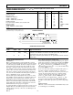
TIMING CHARACTERISTICS
1
Parameter Symbol Value Units Condition
Data Setup Time t
1
20 ns min
SCLK Pulsewidth t
2
100 ns min
Data Hold Time t
3
40 ns min
SCLK Pulse Separation t
4
100 ns min
SCLK to PCLK Delay t
5
65 ns min
SCLK to PCLK Delay and Release (t
5
+ t
6
) 5 ms max
PCLK Pulsewidth t
6
65 ns min
Propagation Delay, PCLK to Switches On or Off _ 70 ns max
Data Load Time _ 52 µs SCLK = 5 MHz
SCLK Frequency _ 20 kHz min
SCLK, PCLK Rise and Fall Times _ 1 µs max
NOTES
1
Timing measurement reference level is 1.5 V.
Specifications subject to change without notice.
OPERATION TRUTH TABLE
Control Lines
PCLK SCLK SIN SOUT Operation/Comment
1 0 X X No operation.
1 1 Data
i
Data
i-256
The data on the SIN line is loaded into the serial register; data clocked into the
serial register 256 clocks ago appears at the SOUT output.
0 X X X Data in the serial shift register transfers into the parallel latches which control the
switch array.
APPLICATIONS INFORMATION
Loading Data
Data to control the switches is clocked serially into a 256-bit
shift register and then transferred in parallel to 256 bits of mem-
ory. The rising edge of SCLK, the serial clock input, loads data
into the shift register. The first bit loaded via SIN, the serial
data input, controls the switch at the intersection of row Y15
and column X15. The next bits control the remaining columns
(down to X0) of row Y15, and are followed by the bits for row
Y14, and so on down to the data for the switch at the intersec-
tion of row Y0 and column X0. The shift register is dynamic, so
there is a minimum clock rate, specified as 20 kHz.
After the shift register is filled with the new 256 bits of control
data, PCLK is activated (pulsed low) to transfer the data to the
parallel latches. Since the shift register is dynamic, there is a
maximum time delay specified before the data is lost: PCLK
must be activated and brought back high within 5 ms after fill-
ing the shift register. The switch control latches are static and
will hold their data as long as power is applied.
To extend the number of switches in the array, you may cascade
multiple AD75019s. The SOUT output is the end of the shift
register, and may be directly connected to the SIN input of the
next AD75019.
Power Supply Sequencing and Bypassing
All junction-isolated parts operating on multiple power supplies
require proper attention to supply sequencing. Because BiMOS
II is a junction-isolated process, parasitic diodes exist between
V
DD
and V
CC
, and between V
SS
and DGND. As a result, V
DD
must always be greater than (V
CC
– 0.5 V), and V
SS
must always
be less than (DGND + 0.5 V).
If you can’t ensure that system power supplies will sequence to
meet these conditions, external Schottky (e.g., 1N5818) or
silicon (e.g., 1N4001) diodes may be used. To protect the posi-
tive side, the anode would connect to V
CC
(Pin 42) and the
cathode to V
DD
(Pin 41). For the negative side, connect the
anode to V
SS
(Pin 4) and the cathode to DGND (Pin 43).
Each of the three power supply pins [V
DD
(Pin 41), V
CC
(Pin
42) and V
SS
(Pin 4)] should be bypassed to DGND (Pin 43)
through a 0.1 µF ceramic capacitor located close to the package
pins.
Transistor Count
AD75019 contains 5,472 transistors. This number may be used
for calculating projected reliability.
TIMING DIAGRAM
Y0–X0Y15–X14
t
6
Y15–X15
t
2
1
0
1
0
SCLK
PCLK
1 = CLOSE
0 = OPEN
SIN
TRANSFER DATA FROM SERIAL
REGISTER TO PARALLEL
LATCHES DURING LOW LEVEL
t
5
t
1
t
3
t
4
LOAD DATA INTO
SERIAL REGISTER
DURING RISING EDGE