
Datasheet

AD7569/AD7669
–11–
REV. B
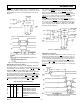
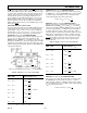
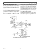
RESET line, the DAC output resets to 0 V when the entire
system is reset. Figure 7 shows the input control logic for the
AD7569 DAC; the write cycle timing diagram is shown in
Figure 8.
Figure 7. AD7569 DAC Input Control Logic
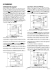
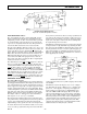
Figure 8. AD7569/AD7669 Write Cycle Timing Diagram
DAC Timing and Control—AD7669
Table III shows the truth table for the dual DAC operation of
the AD7669. The part contains two 8-bit DAC registers that are
loaded from the data bus under the control of
CS, A/B and WR.
Address line
A/B selects which DAC register the data is
loaded to. The data contained in the DAC registers determines
the analog output from the respective DACs. The
WR input is
an edge-triggered input, and data is transferred into the selected
DAC register on the rising edge of
WR. Holding CS and WR
low does not make the selected DAC register transparent. The
A/B input should not be changed while CS and WR are low.
Table III. AD7669 DAC Truth Table
CS WR A/B RESET DAC Function
H H X H DAC Registers Unaffected
L g L H DACA Register Updated
g L L H DACA Register Updated
L g H H DACB Register Updated
g L H H DACB Register Updated
X X X L DAC Registers Loaded with
All Zeros
L = Low State, H = High State, X = Don’t Care
The contents of the DAC registers are reset to all 0s by an active
low pulse on the
RESET line, and for the unipolar output
ranges, the outputs remain at 0 V after
RESET returns high.
For the bipolar output ranges, a low pulse on
RESET causes the
outputs to go to negative full scale. In unipolar applications, the
RESET line can be used to ensure power-up to 0 V on the
AD7669 DAC outputs and is also useful when used as a zero
override in system calibration cycles. If the
RESET input is con-
nected to the system
RESET line, then the DAC outputs reset
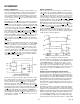
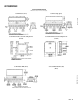
to 0 V when the entire system is reset. Figure 9 shows the DAC
input control logic for the AD7669, and the write cycle timing
diagram is shown in Figure 8.
Figure 9. AD7669 DAC Control Logic
ADC Timing and Control
The ADC on the AD7569/AD7669 is capable of two basic oper-
ating modes. In the first mode, the
ST line is used to start con-
version and drive the track-and-hold into hold mode. At the end
of conversion, the track-and-hold returns to its tracking mode.
The second mode is achieved by hard-wiring the
ST line high.
In this case,
CS and RD start conversion, and the microproces-
sor is driven into a WAIT state for the duration of conversion by
BUSY.
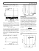
Figure 10. ADC Mode 1 Interface Timing