
Datasheet


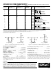


DAC SPECIFICATIONS
1
AD7569
J, A Versions
3
AD7569
AD7669 K, B AD7569 AD7569
Parameter J Version Versions S Version T Version Units Conditions/Comments
STATIC PERFORMANCE
Resolution
4
8 8 8 8 Bits
Total Unadjusted Error
5
±2 ±2 ±3 ±3 LSB typ
Relative Accuracy
5
±1 ±1/2 ±1 ±1/2 LSB max
Differential Nonlinearity
5
±1 ±3/4 ±1 ±3/4 LSB max Guaranteed Monotonic
Unipolar Offset Error DAC data is all 0s; V
SS
= 0 V
@ +25°C ±2 ±1.5 ±2 ±1.5 LSB max Typical tempco is 10 µV/°C for +1.25 V range
T
MIN
to T
MAX
±2.5 ±2 ±2.5 ±2 LSB max
Bipolar Zero Offset Error DAC data is all 0s; V
SS
= –5 V
@ +25°C ±2 ±1 5 ±2 ±1.5 LSB max Typical tempco is 20 µV/°C for ±1.25 V range
T
MIN
to T
MAX
±2.5 ±2 ±2.5 ±2 LSB max
Full-Scale Error
6
(AD7569 Only) V
DD
= 5 V
@ +25°C ±2 ±1 ±2 ±1 LSB max
T
MIN
to T
MAX
±3 ±2 ±4 ±3 LSB max
Full-Scale Error
6
(AD7669 Only) V
DD
= 5 V
@ +25°C ±3 LSB max
T
MIN
to T
MAX
±4.5 LSB max
DACA/DACB Full-Scale Error Match
6
(AD7669 Only) ±2.5 LSB max V
DD
= 5 V
∆Full Scale/∆V
DD
, T
A
= +25°C 0.5 0.5 0.5 0.5 LSB max V
OUT
= 2.5 V; ∆V
DD
= ±5%
∆Full Scale/∆V
SS
, T
A
= +25°C 0.5 0.5 0.5 0.5 LSB max V
OUT
= –2.5 V; ∆V
SS
= ±5%
Load Regulation at Full Scale 0.2 0.2 0.2 0.2 LSB max R
L
= 2 kΩ to °/C
DYNAMIC PERFORMANCE
Signal-to-Noise Ratio
5
(SNR) 44 46 44 46 dB min V
OUT
= 20 kHz full-scale sine wave with f
SAMPLING
= 400 kHz
Total Harmonic Distortion
5
(THD) 48 48 48 48 dB max V
OUT
= 20 kHz full-scale sine wave with f
SAMPLING
= 400 kHz
Intermodulation Distortion
5
(IMD) 55 55 55 55 dB typ fa = 18.4 kHz, fb = 14.5 kHz with f
SAMPLING
= 400 kHz
ANALOG OUTPUT
Output Voltage Ranges
Unipolar 0 to +1.25/2.5 Volts V
DD
= +5 V, V
SS
= 0 V
Bipolar ±1.25/±2.5 Volts V
DD
= +5 V, V
SS
= –5 V
LOGIC INPUTS
CS, X/B,WR, RANGE, RESET, DB0–DB7
Input Low Voltage, V
INL
0.8 0.8 0.8 0.8 V max
Input High Voltage, V
INH
2.4 2.4 2.4 2.4 V min
Input Leakage Current 10 10 10 10 µA max V
IN
= 0 to V
DD
Input Capacitance
7
10 10 10 10 pF max
DB0–DB7
Input Coding (Single Supply) Binary
Input Coding (Dual Supply) 2s Complement
AC CHARACTERlSTICS
7
Voltage Output Settling Time Settling time to within ±1/2 LSB of final value
Positive Full-Scale Change 2 2 2 2 µs max Typically 1 µs
Negative Full-Scale Change (Single Supply) 4 4 4 4 µs max Typically 2 µs
Negative Full-Scale Change (Dual Supply) 2 2 2 2 µs max Typically 1 µs
Digital-to-Analog Glitch Impulse
5
15 15 15 15 nV secs typ
Digital Feedthrough
5
1 1 1 1 nV secs typ
V
IN
to V
OUT
Isolation 60 60 60 60 dB typ V
IN
= ±2.5 V, 50 kHz Sine Wave
DAC to DAC Crosstalk
5
(AD7669 Only) 1 nV secs typ
DACA to DACB Isolation
5
(AD7669 Only) –70 dB max
POWER REQUIREMENTS
V
DD
Range 4.75/5.25 4.75/5.25 4.75/5.25 4.75/5.25 V min/V max For Specified Performance
V
SS
Range (Dual Supplies) –4.75/–5.25 –4.75/–5.25 –4.75/–5.25 –4.75/–5.25 V min/V max Specified Performance also applies to V
SS
= 0 V
for unipolar ranges.
I
DD
V
OUT
= V
IN
= 2.5 V; Logic Inputs = 2.4 V; CLK = 0.8 V
(AD7569) 13 13 13 13 mA max Output unloaded
(AD7669) 18 mA max Outputs unloaded
I
SS
(Dual Supplies) V
OUT
= V
IN
= –2.5 V; Logic Inputs = 2.4 V; CLK = 0.8 V
(AD7569) 4 4 4 4 mA max Output unloaded
(AD7669) 6 mA max Outputs unloaded
DAC/ADC MATCHING
Gain Matching
6
V
IN
to V
OUT
match with V
IN
= ±2.5 V,
@ +25°C 1 111% typ20 kHz sine wave
T
MIN
to T
MAX
1 111% typ
NOTES
1
Specifications apply to both DACs in the AD7669. V
OUT
applies to both V
OUT
A and V
OUT
B of the AD7669.
2
Except where noted, specifications apply for all output ranges including bipolar ranges with dual supply operation.
3
Temperature ranges as follows: J, K versions; 0°C to +70°C
A, B versions; –40°C to +85°C
S, T versions; –55°C to +125°C
4
1 LSB = 4.88 mV for 0 V to +1.25 V output range, 9.76 mV for 0 V to +2.5 V and ±1.25 V ranges and 19.5 mV for ±2.5 V range.
5
See Terminology.
6
Includes internal voltage reference error and is calculated after offset error has been adjusted out. Ideal unipolar full-scale voltage is (FS – 1 LSB); ideal bipolar positive full-scale voltage is (FS/2 – 1 LSB)
and ideal bipolar negative full-scale voltage is –FS/2.
7
Sample tested at +25°C to ensure compliance.
Specifications subject to change without notice.
–2–
REV. B
AD7569/AD7669–SPECIFICATIONS
(V
DD
= +5 V 6 5%; V
SS
2
= RANGE = AGND
DAC
= AGND
ADC
= DGND = 0 V; R
L
= 2 kV, C
L
= 100 pF to AGND
DAC
unless otherwise noted. All specifications T
MIN
to T
MAX
unless otherwise noted.)