
Datasheet


AD7569/AD7669
–7–
REV. B
PIN FUNCTION DESCRIPTION
(Applies to the AD7569 and AD7669 unless otherwise stated.)
Pin
Mnemonic Description
AGND
DAC
Analog Ground for the DAC(s). Separate
ground return paths are provided for the
DAC(s) and ADC to minimize crosstalk.
V
OUT
Output Voltage. V
OUT
is the buffered output
(V
OUT
A, V
OUT
B) voltage from the AD7569 DAC. V
OUT
A and
V
OUT
B are the buffered DAC output voltages
from the AD7669. Four different output volt-
age ranges can be achieved (see Table I).
V
SS
Negative Supply Voltage (–5 V for dual sup-
ply or 0 V for single supply). This pin is also
used with the RANGE pin to select the differ-
ent input/output ranges and changes the data
format from binary (V
SS
= 0 V) to 2s comple-
ment (V
SS
= –5 V) (see Table I).
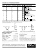
RANGE Range Selection Input. This is used with the
V
SS
input to select the different ranges as per
Table I. The range selected applies to both
the analog input voltage of the ADC and the
output voltage from the DAC(s).
RESET Reset Input (Active Low). This is an asyn-
chronous system reset that clears the DAC
register(s) to all 0s and clears the
INT line of
the ADC (i.e., makes the ADC ready for new
conversion). In unipolar operation, this input
sets the output voltage to 0 V; in bipolar
operation, it sets the output to negative full
scale.
DB7 Data Bit 7. Most Significant Bit (MSB).
DB6–DB2 Data Bit 6 to Data Bit 2.
DGND Digital Ground.
DB1 Data Bit 1.
DB0 Data Bit 0. Least Significant Bit (LSB).
WR Write Input (Edge triggered). This is used in
conjunction with
CS to write data into the
AD7569 DAC register. It is used in conjunc-
tion with
CS and A/B to write data into the
selected DAC register of the AD7669. Data is
transferred on the rising edge of WR.
Pin
Mnemonic Description
CS Chip Select Input (Active Low). The device is
selected when this input is active.
RD READ Input (Active Low). This input must
be active to access data from the part. In the
Mode 2 interface,
RD going low starts con-
version. It is used in conjunction with the
CS
input (see Digital Interface Section).
ST Start Conversion (Edge triggered). This is
used when precise sampling is required. The
falling edge of
ST starts conversion and drives
BUSY low. The ST signal is not gated with
CS.
BUSY BUSY Status Output (Active Low). When
this pin is active, the ADC is performing a
conversion. The input signal is held prior to
the falling edge of
BUSY (see Digital Inter-
face Section).
INT INTERRUPT Output (Active Low). INT go-
ing low indicates that the conversion is com-
plete.
INT goes high on the rising edge of CS
or
RD and is also set high by a low pulse on
RESET (see Digital Interface Section).
A/B (AD7669 DAC Select Input. This input selects which
Only) DAC register data is written to under control
of
CS and WR. With this input low, data is
written to the DACA register; with this input
high, data is written to the DACB register.
CLK A TTL compatible clock signal may be used
to determine the ADC conversion time. Inter-
nal clock operation is achieved by connecting
a resistor and capacitor to ground.
AGND
ADC
Analog Ground for the ADC.
V
IN
Analog Input. Various input ranges can be se-
lected (see Table I).
V
DD
Positive Supply Voltage (+5 V).
Table I. Input/Output Ranges
Input/Output DB0–DB7
Range V
SS
Voltage Range Data Format
0 0 V 0 V to +1.25 V Binary
1 0 V 0 V to +2.5 V Binary
0 –5 V ±1.25 V 2s Complement
1 –5 V ±2.5 V 2s Complement