
Datasheet


Data Sheet AD780
Rev. F | Page 3 of 12
SPECIFICATIONS
T
A
= 25°C, V
IN
= 5 V, unless otherwise noted.
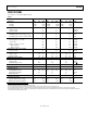
Table 1.
AD780AN/AD780AR AD780CR AD780BN/AD780BR
Parameter Min Typ Max Min Typ Max Min Typ Max Unit
OUTPUT VOLTAGE
2.5 V Out 2.495 2.505 2.4985 2.5015 2.499 2.501 V
3.0 V Out 2.995 3.005 2.9950 3.0050 2.999 3.001 V
OUTPUT VOLTAGE DRIFT
1
−40°C to +85°C 7 7 3 ppm/°C
−55°C to +125°C 20 20 ppm/°C
LINE REGULATION
2.5 V Output, 4 V ≤+V
IN
≤ 36 V, T
MIN
to T
MAX
10 10 10 µV/V
3.0 V Output, 4.5 V ≤+V
IN
≤ 36 V, T
MIN
to T
MAX
10 10 10 µV/V
LOAD REGULATION, SERIES MODE
Sourcing 0 mA < I
OUT
< 10 mA 50 50 50 µV/mA
T
MIN
to T
MAX
75 75 75 µV/mA
Sinking −10 mA < I
OUT
< 0 mA 75 75 75 µV/mA
−40°C to +85°C
75
75
75
µV/mA
−55°C to +125°C 150 150 150 µV/mA
LOAD REGULATION, SHUNT MODE
I < I
SHUNT
< 10 mA 75 75 75 µV/mA
QUIESCENT CURRENT, 2.5 V SERIES MODE
2
–40°C to +85°C 0.75 1.0 0.75 1.0 0.75 1.0 mA
−55°C to +125°C 0.8 1.3 0.8 1.3 0.8 1.3 mA
MINIMUM SHUNT CURRENT 0.7 1.0 0.7 1.0 0.7 1.0 mA
OUTPUT NOISE
0.1 Hz to 10 Hz 4 4 4 µV p-p
Spectral Density, 100 Hz 100 100 100 nV/√
Hz
LONG-TERM STABILITY
3
20 20 20 ± ppm/1000 Hr
TRIM RANGE 4.0 4.0 4.0 ± %
TEMPERATURE PIN
Voltage Output @ 25°C 500 560 620 500 560 620 500 560 620 mV
Temperature Sensitivity 1.9 1.9 1.9 mV/°C
Output Resistance 3 3 3 kΩ
SHORT-CIRCUIT CURRENT TO GROUND 30 30 30 mA
TEMPERATURE RANGE
Specified Performance (A, B, C)
–40
+85
–40
+85
–40
+85
°C
Operating Performance (A, B, C)
4
–55 +125 –55 +125 –55 +125 °C
1
Maximum output voltage drift is guaranteed for all packages.
2
3.0 V mode typically adds 100 µA to the quiescent current. Also, Iq increases by 2 µA/V above an input voltage of 5 V.
3
The long-term stability specification is noncumulative. The drift in subsequent 1,000 hour periods is significantly lower than in the first 1,000 hour period.
4
The operating temperature range is defined as the temperature extremes at which the device will still function. Parts may deviate from their specified performance
outside their specified temperature range.