
Datasheet


Data Sheet AD780
Rev. F | Page 7 of 12
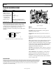
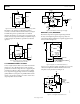
00841-009
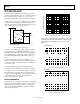
NC
TEMP
+V
IN
V
OUT
TRIM
GND
O/P SELECT
2.5V – NC
3.0V – GND
NC
1F
AD780
NC = NO CONNECT
1
7
6
5
84
2
3
C2
C1
Figure 9. Noise Reduction Circuit
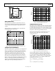
NOISE COMPARISON
The wideband noise performance of the AD780 can also be
expressed in ppm. The typical performance with C1 and C2 is
0.6 ppm; without external capacitors, typical performance is
1.2 ppm.
This performance is, respectively, 7× and 3× lower than the
specified performance of the LT1019.
00841-010
10Hz TO 10kHz
NO AMPLIFIER
10ms20V
100
90
10
0%
Figure 10. Reduced Noise Performance with C1 = 100 μF, C2 = 100 nF
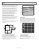
TEMPERATURE PERFORMANCE
The AD780 provides superior performance over temperature by
means of a combination of patented circuit design techniques,
precision thin-film resistors, and drift trimming. Temperature
performance is specified in terms of ppm/°C; because of
nonlinearity in the temperature characteristic, the box test
method is used to test and specify the part. The nonlinearity
takes the form of the characteristic S-shaped curve shown in
Figure 11. The box test method forms a rectangular box around
this curve, enclosing the maximum and minimum output
voltages over the specified temperature range. The specified
drift is equal to the slope of the diagonal of this box.
2.0
–0.8
–0.4
0
0.4
0.8
1.2
1.6
–60 –40 –20 0 20 40 60 80 100 120 140
00841-011
TEMPERATURE (C)
ERROR (mV)
Figure 11. Typical AD780BN Temperature Drift
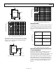
TEMPERATURE OUTPUT PIN
The AD780 provides a TEMP output (Pin 3) that varies linearly
with temperature. This output can be used to monitor changes
in system ambient temperature, and to initiate calibration of the
system, if desired. The voltage V
TEMP
is 560 mV at 25°C, and the
temperature coefficient is approximately 2 mV/°C.
Figure 12 shows the typical V
TEMP
characteristic curve over
temperature taken at the output of the op amp with a
noninverting gain of 5.
4.25
4.00
3.75
3.50
3.25
3.00
2.75
2.50
2.25
2.00
–75 –50 –25 0 25 50 75 100 125 150
00841-012
TEMPERATURE (C)
VOLTAGE (V
OUT
)
CIRCUIT CALIBRATED AT 25C
REFER TO FIGURE 13
10mV PER C
Figure 12. Temperature Pin Transfer Characteristic
Since the TEMP voltage is acquired from the band gap core
circuit, current pulled from this pin has a significant effect on
V
OUT
. Care must be taken to buffer the TEMP output with a
suitable op amp, e.g., an OP07, AD820, or AD711 (all of which
would result in less than a 100 μV change in VOUT). The
relationship between I
TEMP
and V
OUT
is
ΔV
OUT
= 5.8 mV/μA I
TEMP
(2.5 V Range)
or
ΔV
OUT
= 6.9 mV/μA I
TEMP
(3.0 V Range)