
Datasheet


AD780 Data Sheet
Rev. F | Page 8 of 12
Notice how sensitive the current dependent factor on V
OUT
is. A
large amount of current, even in tens of microamp, drawn from
the TEMP pin can cause the V
OUT
and TEMP output to fail.
The choice of C1 and C2 was dictated primarily by the need for
a relatively flat response that rolled off early in the high
frequency noise at the output. However, there is considerable
margin in the choice of these capacitors. For example, the user
can actually put a huge C2 on the TEMP pin with none on the
output pin. However, one must either put very little or a lot of
capacitance at the TEMP pin. Intermediate values of
capacitance can sometimes cause oscillation. In any case, the
user should follow the recommendation in Figure 6.
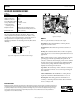
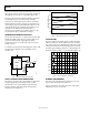
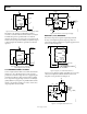
TEMPERATURE TRANSDUCER CIRCUIT
The circuit shown in Figure 13 is a temperature transducer that
amplifies the TEMP output voltage by a gain of a little over +5
to provide a wider full-scale output range. The digital
potentiometer can be used to adjust the output so it varies by
exactly 10 mV/°C.
To minimize resistance changes with temperature, resistors with
low temperature coefficients, such as metal film resistors,
should be used.
00841-013
AD780
GND
R
B
1.27kΩ
(1%)
R
F
6.04k
Ω (1%)
4
+V
IN
2
3
1µF
TEMP
R
BP
200Ω
AD820
10mV/°C
5V
Figure 13. Differential Temperature Transducer
SUPPLY CURRENT OVER TEMPERATURE
The AD780’s quiescent current varies slightly over temperature
and input supply range. The test limit is 1 mA over the
industrial and 1.3 mA over the military temperature range.
Typical performance with input voltage and temperature
variation is shown in Figure 14.
0.85
0.80
0.75
0.70
0.65
0.60
4 36
00841-014
INPUT VOLTAGE (V)
QUIESCENT CURRENT (mA)
–55°C
+25°C
+125°C
Figure 14. Typical Supply Current over Temperature
TURN-ON TIME
The time required for the output voltage to reach its final value
within a specified error band is defined as the turn-on settling
time. The two major factors that affect this are the active circuit
settling time and the time for the thermal gradients on the chip
to stabilize. Typical settling performance is shown in Figure 15.
The AD780 settles to within 0.1% of its final value within 10 µs.
5V
0V
2.500V
2.499V
2.498V
00841-015
10
µs/DIV
V
IN
V
OUT
Figure 15. Turn-On Settling Time Performance
DYNAMIC PERFORMANCE
The output stage of the AD780 has been designed to provide
superior static and dynamic load regulation.
Figure 16 and Figure 17 show the performance of the AD780
while driving a 0 mA to 10 mA load.