
Datasheet

AD780
REV. B
–4–
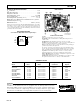
THEORY OF OPERATION
Bandgap references are the high performance solution for low
supply voltage and low power voltage reference applications. In
this technique a voltage with a positive temperature coefficient is
combined with the negative coefficient of a transistor’s Vbe to
produce a constant bandgap voltage.
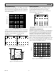
In the AD780, the bandgap cell contains two npn transistors
(Q6 and Q7) which differ in emitter area by 12⫻. The differ-
ence in their Vbe’s produces a PTAT current in R5. This in
turn produces a PTAT voltage across R4, which when com-
bined with the Vbe of Q7, produces a voltage Vbg that does not
vary with temperature. Precision laser trimming of the resistors
and other patented circuit techniques are used to further enhance
the drift performance.
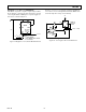
NC
TEMP
+V
IN
V
OUT
TRIM
GND
O/P SELECT
2.5V - NC
3.0V - GND
Q6
Q7
R10
R11
R5
R4
R14 R15
R16
R13
NC = NO CONNECT
NC
AD780
Figure 1. Schematic Diagram
The output voltage of the AD780 is determined by the configu-
ration of resistors R13, R14 and R15 in the amplifier’s feedback
loop. This sets the output to either 2.5 V or 3.0 V depending on
whether R15 (Pin 8) is grounded or not connected.
A unique feature of the AD780 is the low headroom design of
the high gain amplifier which produces a precision 3 V output
from an input voltage as low as 4.5 V (or 2.5 V from a 4.0 V
input). The amplifier design also allows the part to work with
V
IN
= V
OUT
when current is forced into the output terminal.
This allows the AD780 to work as a two terminal shunt regula-
tor providing a –2.5 V or –3.0 V reference voltage output with-
out external components.
The PTAT voltage is also used to provide the user with a ther-
mometer output voltage (at Pin 3) which increases at a rate of
approximately 2 mV/°C.
The AD780’s NC Pin 7 is a 20 kΩ resistor to V+ which is used
solely for production test purposes. Users who are currently us-
ing the LT1019 self-heater pin (Pin 7) must take into account
the different load on the heater supply.
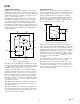
APPLYING THE AD780
The AD780 can be used without any external components to
achieve specified performance. If power is supplied to Pin 2 and
Pin 4 is grounded, Pin 6 provides a 2.5 V or 3.0 V output de-
pending on whether Pin 8 is left unconnected or grounded.
A bypass capacitor of 1 µF (V
IN
to GND) should be used if the
load capacitance in the application is expected to be greater
than 1 nF. The AD780 in 2.5 V mode typically draws 700 µA of
Iq at 5 V. This increases by ~2 µA/V up to 36 V.
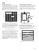
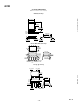
NC
TEMP
+V
IN
V
OUT
TRIM
GND
O/P SELECT
2.5V – NC
3.0V – GND
NC
R
NULL
R POT.
1F
AD780
NC = NO CONNECT
Figure 2. Optional Fine Trim Circuit
Initial error can be nulled using a single 25 kΩ potentiometer
connected between V
OUT
, Trim and GND. This is a coarse trim
with an adjustment range of ±4% and is only included here for
compatibility purposes with other references. A fine trim can be
implemented by inserting a large value resistor (e.g. 1–5 MΩ) in
series with the wiper of the potentiometer. See Figure 2 above.
The trim range, expressed as a fraction of the output, is simply
greater than or equal to 2.1 kΩ/R
NULL
for either the 2.5 V or
3.0 V mode.
The external null resistor affects the overall temperature coeffi-
cient by a factor equal to the percentage of V
OUT
nulled.
For example a 1 mV (.03%) shift in the output caused by the
trim circuit, with a 100 ppm/°C null resistor will add less than
0.06 ppm/°C to the output drift (0.03% ⫻ 200 ppm/°C, since
the resistors internal to the AD780 also have temperature coeffi-
cients of less than 100 ppm/°C).