
Datasheet

AD780
REV. B
–7–
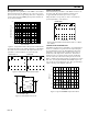
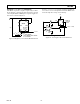
TURN-ON TIME
The time required for the output voltage to reach its final value
within a specified error band is defined as the turn-on settling
time. The two major factors that affect this are the active circuit
settling time and the time for the thermal gradients on the chip
to stabilize. Typical settling performance is shown in Figure 11
following. The AD780 settles to within 0.1% of its final value
within 10 µs.
2.499V
2.498V
2.500V
0V
5V
10s/DIV
V
IN
V
OUT
Figure 11. Turn-On Settling Time Performance
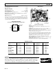
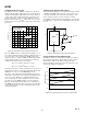
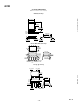
DYNAMIC PERFORMANCE
The output stage of the AD780 has been designed to provide
superior static and dynamic load regulation.
Figure 12 shows the performance of the AD780 while driving a
0 mA to 10 mA load.
+V
IN
V
OUT
AD780
V
L
0V
V
OUT
249
1F
Figure 12a. Transient Resistive Load Test Circuit
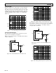
OUTPUT CHANGE – 50mV/DIV
10mA
0mA
10s/DIV
I
LOAD
V
OUT
(C
L
= 0pF)
Figure 12b. Settling Under Transient Resistive Load
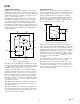
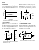
The dynamic load may be resistive and capacitive. For example
the load may be connected via a long capacitive cable. Figure 13
following shows the performance of the AD780 driving a
1000 pF, 0 mA to 10 mA load.
+V
IN
V
OUT
AD780
V
L
0V
V
OUT
249
1F
C
L
1000pF
Figure 13a. Capacitive Load Transient Response
Test Circuit
OUTPUT CHANGE – 50mV/DIV
10s/DIV
0mA
10mA
I
LOAD
V
OUT
(C
L
= 1000pF)
Figure 13b. Settling Under Dynamic Capacitive Load