
Datasheet


REV. E
–2–
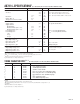
AD7814–SPECIFICATIONS
1
Parameter Min Typ Max Unit Test Conditions/Comments
TEMPERATURE SENSOR AND ADC
Accuracy ± 2.0 °CT
A
= 0°C to 85°C. V
DD
= 3 V to 5.5 V
2
± 2.5 °CT
A
= –40°C to 0°C. V
DD
= 3 V to 5.5 V
2
± 2.0 ± 3.5 °CT
A
= –55°C to +125°C. V
DD
= 3 V to 5.5 V
Resolution 10 Bits
Update Rate, t
R
400 µs
Temperature Conversion Time 25 µs
SUPPLIES
Supply Voltage 2.7 5.5 V For Specified Performance
Supply Current
Normal Mode 250 400 µA
Shutdown Mode (V
DD
= 5 V) 1.23 3 µA
Shutdown Mode (V
DD
= 3 V) 0.43 1 µA
Power Dissipation 80 µWV
DD
= 3 V. Using Normal Mode
Power Dissipation V
DD
= 3 V. Using Shutdown Mode
1 sps 3.7 µW
10 sps 3.9 µW
100 sps 5.8 µW
DIGITAL INPUT
3
Input High Voltage, V
IH
2.4 V
Input Low Voltage, V
IL
0.8 V
Input Current, I
IN
± 1 µAV
IN
= 0 V to V
DD
Input Capacitance, C
IN
10 pF All Digital Inputs
DIGITAL OUTPUT
3
Output High Voltage, V
OH
V
DD
– 0.3 V I
SOURCE
= I
SINK
= 200 µA
Output Low Voltage, V
OL
0.4 V I
OL
= 200 µA
Output Capacitance, C
OUT
50 pF
NOTES
1
All specifications apply for –55°C to +125°C unless otherwise stated.
2
For V
DD
= 2.7 V to 3 V and T
A
= –40°C to +85°C, the typical temperature error is ± 2°C.
3
Guaranteed by design and characterization, not production tested.
Specifications subject to change without notice.
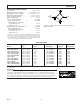
TIMING CHARACTERISTICS
1, 2, 3
Parameter Limit Unit Comments
t
1
0 ns min CS to SCLK Setup Time
t
2
50 ns min SCLK High Pulse Width
t
3
50 ns min SCLK Low Pulse Width
t
4
4
35 ns max Data Access Time After SCLK Falling Edge
t
5
20 ns min Data Setup Time Prior to SCLK Rising Edge
t
6
0 ns min Data Hold Time After SCLK Rising Edge
t
7
0 ns min CS to SCLK Hold Time
t
8
4
40 ns max CS to DOUT High Impedance
NOTES
1
Guaranteed by design and characterization, not production tested.
2
All input signals are specified with tr = tf = 5 ns (10% to 90% of V
DD
) and timed from a voltage level of 1.6 V.
3
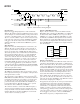
See Figure 2.
4
Measured with the load circuit of Figure 1.
Specifications subject to change without notice.
(T
A
= T
MIN
to T
MAX
, V
DD
= 2.7 V to 5.5 V, unless otherwise noted.)
(T
A
= T
MIN
to T
MAX
, V
DD
= 2.7 V to 5.5 V, unless otherwise noted.)