
Datasheet


AD7869
TIMING SPECIFICATIONS
1, 2
–4–
Limit at T
MIN
, T
MAX
Parameter (All Versions) Units Conditions/Comments
ADC TIMING
t
1
50 ns min CONVST Pulse Width
t
2
3
440 ns min RCLK Cycle Time, Internal Clock
t
3
100 ns min RFS to RCLK Falling Edge Setup Time
t
4
20 ns min RCLK Rising Edge to RFS
100 ns max
t
5
4
155 ns max RCLK to Valid Data Delay, C
L
= 35 pF
t
6
4 ns min Bus Relinquish Time after RCLK
100 ns max
t
13
5
2 RCLK + 200 to ns typ CONVST to RFS Delay
3 RCLK + 200
DAC TIMING
t
7
50 ns min TFS to TCLK Falling Edge
t
8
75 ns min TCLK Falling Edge to TFS
t
9
150 ns min TCLK Cycle Time
t
10
30 ns min Data Valid to TCLK Setup Time
t
11
75 ns min Data Valid to TCLK Hold Time
t
l2
40 ns min LDAC Pulse Width
NOTES
1
Timing specifications are sample tested at +25°C to ensure compliance. All input signals are specified with tr = tf = 5 ns (10% to 90% of 5 V) and timed from a
voltage level of 1.6 V.
2
Serial timing is measured with a 4.7 kΩ pull-up resistor on DR and RFS and a 2 kΩ pull-up resistor on RCLK. The capacitance on all three outputs is 35 pF.
3
When using internal clock, RCLK mark/space ratio (measured form a voltage level of 1.6 V) range is 40/60 to 60/40. For external clock, RCLK mark/space
ratio = external clock mark/space ratio.
4
DR will drive higher capacitance loads but this will add to t
5
since it increases the external RC time constant (4.7 kΩ//C
L
) and hence the time to reach 2.4 V.
5
Time 2 RCLK to 3 RCLK depends on conversion start to ADC clock synchronization.
6
TCLK mark/space ratio is 40/60 to 60/40.
ABSOLUTE MAXIMUM RATINGS*
(T
A
= + 25°C unless otherwise noted)
V
DD
to AGND . . . . . . . . . . . . . . . . . . . . . . . . . –0.3 V to +7 V
V
SS
to AGND . . . . . . . . . . . . . . . . . . . . . . . . . +0.3 V to –7 V
AGND to DGND . . . . . . . . . . . . . . . . –0.3 V to V
DD
+ 0.3 V
V
OUT
to AGND . . . . . . . . . . . . . . . . . . . . . . . . . . . V
SS
to V
DD
V
IN
to AGND . . . . . . . . . . . . . . . . V
SS
–0.3 V to V
DD
+ 0.3 V
RO ADC to AGND . . . . . . . . . . . . . . . –0.3 V to V
DD
+ 0.3 V
RO DAC to AGND . . . . . . . . . . . . . . . –0.3 V to V
DD
+ 0.3 V
RI DAC to AGND . . . . . . . . . . . . . . . –0.3 V to V
DD
+ 0.3 V
Digital Inputs to DGND . . . . . . . . . . . –0.3 V to V
DD
+ 0.3 V
Digital Outputs to DGND . . . . . . . . . . –0.3 V to V
DD
+ 0.3 V
Operating Temperature Range
J Version . . . . . . . . . . . . . . . . . . . . . . . . . . . . 0°C to +70°C
A Version . . . . . . . . . . . . . . . . . . . . . . . . . . –40°C to +85°C
Storage Temperature Range . . . . . . . . . . . . –65°C to +150°C
Lead Temperature (Soldering, 10 secs) . . . . . . . . . . . +300°C
Power Dissipation (Any Package) to +75°C . . . . . . . 1000 mW
Derates above +75°C by . . . . . . . . . . . . . . . . . . . . 10 mW/°C
*Stresses above those listed under “Absolute Maximum Ratings” may cause
permanent damage to the device. This is a stress rating only; functional operation
of the device at these or any other conditions above those listed in the operational
sections of this specification is not implied. Exposure to absolute maximum rating
conditions for extended periods may affect device reliability.
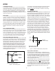
WARNING!
ESD SENSITIVE DEVICE
CAUTION
ESD (electrostatic discharge) sensitive device. Electrostatic charges as high as 4000 V readily
accumulate on the human body and test equipment and can discharge without detection.
Although the AD7869 features proprietary ESD protection circuitry, permanent damage may
occur on devices subjected to high energy electrostatic discharges. Therefore, proper ESD
precautions are recommended to avoid performance degradation or loss of functionality.
(V
DD
= +5 V 6 5%, V
SS
= –5 V 6 5%, AGND = DGND = 0 V)
REV. B