
Datasheet


AD7869
–8–
TIMING AND CONTROL
Communication with the AD7869 is managed by six dedicated
pins. These consist of separate serial clocks, word framing or
strobe pulses, and data signals for both receiving and transmit-
ting data. Conversion starts and DAC updating are controlled
by two digital inputs,
CONVST and LDAC. These inputs can
be asserted independently of the microprocessor by an external
timer when precise sampling intervals are required. Alterna-
tively, the
LDAC and CONVST can be driven from a decoded
address bus, allowing the microprocessor control over conver-
sion start and DAC updating as well as data communication to
the AD7869.
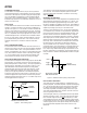
ADC Timing
Conversion control is provided by the CONVST input. A low to
high transition on
CONVST input starts conversion and drives
the track/hold amplifier into its hold mode. Serial data then be-
comes available while conversion is in progress. The corre-
sponding timing diagram is shown in Figure 7. The word length
is 16 bits, two leading zeros followed by the 14-bit conversion
result starting with the MSB. The data is synchronized to the
serial clock output (RCLK) and is framed by the serial strobe
(
RFS). Data is clocked out on a low to high transition of the se-
rial clock and is valid on the falling edge of this clock while the
RFS output is low. RFS goes low at the start of conversion, and
the first serial data bit (which is the first leading zero) is valid on
the first falling edge of RCLK. All the ADC serial lines are
open-drain outputs and require external pull-up resistors.
t
1
t
13
t
3
t
2
t
4
t
6
t
5
CONVST
RFS
1
RCLK
2,3
DR
1
DB13 DB12 DB11 DB1 DB0
CONVERSION TIME
Figure 7. ADC Control Timing Diagram
The serial clock out is derived from the ADC master clock
source, which may be internal or external. Normally, RCLK is
required during the serial transmission only. In these cases, it
can be shut down (i.e., placed into three-state) at the end of
conversion to allow multiple ADCs to share a common serial
bus. However, some serial systems (e.g., TMS32020) require a
serial clock that runs continuously. Both options are available
on the AD7869 ADC. With the CONTROL input at 0 V,
RCLK is noncontinuous; when it is at –5 V, RCLK is
continuous.
DAC TIMING
The AD7869 DAC contains two latches, an input latch and a
DAC latch. Data must be loaded to the input latch under the
control of the TCLK,
TFS and DT serial logic inputs. Data is
then transferred from the input latch to the DAC latch under
the control of the
LDAC signal. Only the data in the DAC latch
determines the analog output of the AD7869.
Data is loaded to the input latch under control of TCLK,
TFS
and DT. The AD7869 DAC expects a 16-bit stream of serial
data on its DT input. Data must be valid on the falling edge of
TCLK. The
TFS input provides the frame synchronization sig-
nal, which tells the AD7869 DAC that valid serial data will be
available for the next 16 falling edges of TCLK. Figure 8 shows
the timing diagram for the serial data format.
DB13 DB12
DB11 DB10 DB1 DB0
t
7
t
8
t
9
t
10
t
11
TFS
TCLK
DT
DON'T
CARE
DON'T
CARE
Figure 8. DAC Control Timing Diagram
Although 16 bits of data are clocked into the input latch, only
14 bits are transferred into the DAC latch. Therefore, two bits
in the stream are don’t cares since their value does not affect the
DAC latch data. The bit positions are two don’t cares, followed
by the 14-bit DAC data starting with the MSB.
The
LDAC signal controls the transfer of data to the DAC
latch. Normally, data is loaded to the DAC latch on the falling
edge of
LDAC. However, if LDAC is held low, then serial data
is loaded to the DAC latch on the sixteenth falling edge of
TCLK. If
LDAC goes low during the loading of serial data to
the input latch, no DAC latch update takes place on the falling
edge of
LDAC. If LDAC stays low until the serial transfer is
completed, the update takes place on the sixteenth falling edge
of TCLK. If
LDAC returns high before the serial data transfer
is completed, no DAC latch update takes place.
REV. B