
Datasheet
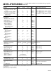

AD7893–SPECIFICATIONS
ABS
Parameter Versions
l
Versions Version Units Test Conditions/Comments
DYNAMIC PERFORMANCE
Signal to (Noise + Distortion) Ratio
2
@ +25°C 70 70 70 dB min f
IN
= 10 kHz Sine Wave, f
SAMPLE
= 117 kHz
Total Harmonic Distortion (THD)
2
–80 –80 –80 dB max f
IN
= 10 kHz Sine Wave, f
SAMPLE
= 117 kHz
Peak Harmonic or Spurious Noise
2
–80 –80 –80 dB max f
IN
= 10 kHz Sine Wave, f
SAMPLE
= 117 kHz
Intermodulation Distortion (IMD)
2
fa = 9 kHz, fb = 9.5 kHz, f
SAMPLE
= 117 kHz
2nd Order Terms –80 –80 –80 dB max
3rd Order Terms –80 –80 –80 dB max
DC ACCURACY
Resolution 12 12 12 Bits
Minimum Resolution for which
No Missing Codes are Guaranteed 12 12 12 Bits
Relative Accuracy
2
±1 ±1/2 ±1 LSB max
Differential Nonlinearity
2
±1 ±1 ±1 LSB max
Positive Full-Scale Error
2
±3 ±1.5 ±3 LSB max
AD7893-2, AD7893-5
Unipolar Offset Error ±4 ±3 ±4 LSB max
AD7893-10, AD7893-3
Negative Full-Scale Error
2
±3 ±1.5 ±3 LSB max
Bipolar Zero Error ±4 ±2 ±4 LSB max
ANALOG INPUT
AD7893-10
Input Voltage Range ±10 ±10 ±10 Volts
Input Resistance 16 16 16 kΩ min
AD7893-3
Input Voltage Range ±2.5 ±2.5 ±2.5 Volts
Input Resistance 4 4 4 kΩ min
AD7893-5
Input Voltage Range 0 to +5 0 to +5 0 to +5 Volts
Input Resistance 9 9 9 kΩ min
AD7893-2
Input Voltage Range 0 to +2.5 0 to +2.5 0 to +2.5 Volts
Input Current 500 500 500 nA max
REFERENCE INPUT
REF IN Input Voltage Range 2.375/2.625 2.375/2.625 2.375/2.625 V min/V max 2.5 V ± 5%
Input Current 2 2 10 µA max
Input Capacitance
3
10 10 10 pF max
LOGIC INPUTS
Input High Voltage, V
INH
2.4 2.4 2.4 V min V
DD
= 5 V ± 5%
Input Low Voltage, V
INL
0.8 0.8 0.8 V max V
DD
= 5 V ± 5%
Input Current, I
IN
±10 ±10 ±10 µA max V
IN
= 0 V to V
DD
Input Capacitance, C
IN
3
10 10 10 pF max
LOGIC OUTPUTS
Output High Voltage, V
OH
4.0 4.0 4.0 V min I
SOURCE
= 200 µA
Output Low Voltage, V
OL
0.4 0.4 0.4 V max I
SINK
= 1.6 mA
Output Coding
AD7893-10, AD7893-3 2s Complement
AD7893-2, AD7893-5 Straight (Natural) Binary
CONVERSION RATE
Conversion Time 6 6 6 µs max
Track/Hold Acquisition Time
2
1.5 1.5 1.5 µs max
POWER REQUIREMENTS
V
DD
+5 +5 +5 V nom ±5% for Specified Performance
I
DD
9 9 9 mA max
Power Dissipation 45 45 45 mW max Typically 25 mW
NOTES
1
Temperature Ranges are as follows: A, B Versions: –40°C to +85°C, S Version: –55°C to +125°C.
2
See Terminology.
3
Sample tested @ +25°C to ensure compliance.
Specifications subject to change without notice.
REV. E
–2–
(V
DD
= +5 V, AGND = DGND = 0 V, REF IN = +2.5 V. All specifications T
MIN
to T
MAX
unless
otherwise noted.)