
Datasheet
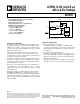

AD7893
–3–
REV. E
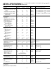
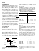
TIMING CHARACTERISTICS
1, 2
A, B S
Parameter Versions Version Units Test Conditions/Comments
t
1
50 50 ns min CONVST Pulse Width
t
2
60 70 ns min SCLK High Pulse Width
t
3
30 40 ns min SCLK Low Pulse Width
t
4
3
50 60 ns max SCLK Rising Edge to Data Valid Delay
t
5
4
10 10 ns min Bus Relinquish Time after Falling Edge of SCLK
100 100 ns max
NOTES
1
Sample tested at +25°C to ensure compliance. All input signals are measured with tr = tf = 1 ns (10% to 90% of +5 V) and timed from a voltage level of +1.6 V.
2
See Figure 5.
3
Measured with the load circuit of Figure 1 and defined as the time required for an output to cross 0.8 V or 2.4 V.
4
Derived from the measured time taken by the data outputs to change 0.5 V when loaded with the circuit of Figure 1. The measured number is then extrapolated back
to remove the effects of charging or discharging the 50 pF capacitor. This means that the time, t
5
, quoted in the timing characteristics is the true bus relinquish time
of the part and, as such, is independent of external bus loading capacitances.
(V
DD
= +5 V, AGND = DGND = 0 V, REF IN = +2.5 V)
ABSOLUTE MAXIMUM RATINGS*
(T
A
= +25°C unless otherwise noted)
V
DD
to AGND . . . . . . . . . . . . . . . . . . . . . . . . . –0.3 V to +7 V
V
DD
to DGND . . . . . . . . . . . . . . . . . . . . . . . . . –0.3 V to +7 V
Analog Input Voltage to AGND
AD7893-10, AD7893-5 . . . . . . . . . . . . . . . . . . . . . . . ±17 V
AD7893-2, AD7893-3 . . . . . . . . . . . . . . . . . . . –5 V, +10 V
Reference Input Voltage to AGND . . . –0.3 V to V
DD
+ 0.3 V
Digital Input Voltage to DGND . . . . . –0.3 V to V
DD
+ 0.3 V
Digital Output Voltage to DGND . . . . –0.3 V to V
DD
+ 0.3 V
Operating Temperature Range
Commercial (A, B Versions) . . . . . . . . . . . –40°C to +85°C
Extended (S Version) . . . . . . . . . . . . . . . . –55°C to +125°C
Storage Temperature Range . . . . . . . . . . . . –65°C to +150°C
Junction Temperature . . . . . . . . . . . . . . . . . . . . . . . . . +150°C
Plastic DIP Package, Power Dissipation . . . . . . . . . . 450 mW
θ
JA
Thermal Impedance . . . . . . . . . . . . . . . . . . . . . 130°C/W
Lead Temperature (Soldering, 10 sec) . . . . . . . . . . . +260°C
Cerdip Package, Power Dissipation . . . . . . . . . . . . . . 450 mW
θ
JA
Thermal Impedance . . . . . . . . . . . . . . . . . . . . . 125°C/W
Lead Temperature (Soldering, 10 sec) . . . . . . . . . . . +300°C
SOIC Package, Power Dissipation . . . . . . . . . . . . . . . 450 mW
θ
JA
Thermal Impedance . . . . . . . . . . . . . . . . . . . . . 170°C/W
Lead Temperature, Soldering
Vapor Phase (60 sec) . . . . . . . . . . . . . . . . . . . . . . +215°C
Infrared (15 sec) . . . . . . . . . . . . . . . . . . . . . . . . . . +220°C
*Stresses above those listed under “Absolute Maximum Ratings” may cause
permanent damage to the device. This is a stress rating only; functional operation
of the device at these or any other conditions above those listed in the operational
sections of this specification is not implied. Exposure to absolute maximum rating
conditions for extended periods may affect device reliability.
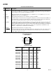
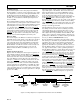
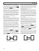
TO
OUTPUT
PIN
+2.1V
1.6mA
200µA
50pF
Figure 1. Load Circuit for Access Time and Bus
Relinquish Time
WARNING!
ESD SENSITIVE DEVICE
CAUTION
ESD (electrostatic discharge) sensitive device. Electrostatic charges as high as 4000 V readily
accumulate on the human body and test equipment and can discharge without detection. Although
the AD7893 features proprietary ESD protection circuitry, permanent damage may occur on devices
subjected to high energy electrostatic discharges. Therefore, proper ESD precautions are
recommended to avoid performance degradation or loss of functionality.