
Datasheet

AD7893
REV. E
–4–
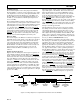
PIN FUNCTION DESCRIPTION
Pin Pin
No. Mnemonic Description
1 REF IN Voltage Reference Input. An external reference source should be connected to this pin to provide the refer-
ence voltage for the AD7893’s conversion process. The REF IN input is buffered on-chip. The nominal ref-
erence voltage for correct operation of the AD7893 is +2.5 V.
2V
IN
Analog Input Channel. The analog input range is ±10 V (AD7893-10), ±2.5 V (AD7893-3), 0 V to +5 V
(AD7893-5) and 0 V to +2.5 V (AD7893-2).
3 AGND Analog Ground. Ground reference for track/hold, comparator and DAC.
4 SCLK Serial Clock Input. An external serial clock is applied to this input to obtain serial data from the AD7893. A
new serial data bit is clocked out on the rising edge of this serial clock, and data is valid on the falling edge.
The serial clock input should be taken low at the end of the serial data transmission.
5 SDATA Serial Data Output. Serial data from the AD7893 is provided at this output. The serial data is clocked out by
the rising edge of SCLK and is valid on the falling edge of SCLK. Sixteen bits of serial data are provided
with four leading zeros followed by the 12 bits of conversion data. On the sixteenth falling edge of SCLK, the
SDATA line is disabled (three-stated). Output data coding is twos complement for the AD7893-10 and
AD7893-3, straight binary for the AD7893-2 and AD7893-5.
6 DGND Digital Ground. Ground reference for digital circuitry.
7
CONVST Convert Start. Edge-triggered logic input. On the falling edge of this input, the serial clock counter is reset to
zero. On the rising edge of this input, the track/hold goes into its hold mode and conversion is initiated.
8V
DD
Positive supply voltage, +5 V ± 5%.
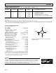
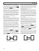
PIN CONFIGURATION
DIP and SOIC
1
2
3
4
8
7
6
5
REF IN
V
IN
AGND
SCLK
DGND
SDATA
V
DD
CONVST
AD7893
TOP VIEW
(NOT TO SCALE)
ORDERING GUIDE
Temperature Linearity Package
Model Range Error SNR Options*
AD7893AN-2 –40°C to +85°C ±1 LSB 70 dB N-8
AD7893BN-2 –40°C to +85°C ±1/2 LSB 72 dB N-8
AD7893AR-2 –40°C to +85°C ±1 LSB 70 dB SO-8
AD7893BR-2 –40°C to +85°C ±1/2 LSB 72 dB SO-8
AD7893SQ-2 –55°C to +125°C ±1 LSB 70 dB Q-8
AD7893AN-5 –40°C to +85°C ±1 LSB 70 dB N-8
AD7893BN-5 –40°C to +85°C ±1/2 LSB 72 dB N-8
AD7893AR-5 –40°C to +85°C ±1 LSB 70 dB SO-8
AD7893BR-5 –40°C to +85°C ±1/2 LSB 72 dB SO-8
AD7893SQ-5 –55°C to +125°C ±1 LSB 70 dB Q-8
AD7893AN-10 –40°C to +85°C ±1 LSB 70 dB N-8
AD7893BN-10 –40°C to +85°C ±1/2 LSB 72 dB N-8
AD7893AR-10 –40°C to +85°C ±1 LSB 70 dB SO-8
AD7893BR-10 –40°C to +85°C ±1/2 LSB 72 dB SO-8
AD7893SQ-10 –55°C to +125°C ±1 LSB 70 dB Q-8
AD7893AR-3 –40°C to +85°C ±1 LSB 70 dB SO-8
*N = Plastic DIP, Q = Cerdip, SO = SOIC.