
Datasheet

4-Channel, 10- and 12-Bit ADCs with I
2
C-
Compatible Interface in 16-Lead TSSOP
AD7993/AD7994
Rev. 0
Information furnished by Analog Devices is believed to be accurate and reliable.
However, no responsibility is assumed by Analog Devices for its use, nor for any
infringements of patents or other rights of third parties that may result from its use.
Specifications subject to change without notice. No license is granted by implication
or otherwise under any patent or patent rights of Analog Devices. Trademarks and
registered trademarks are the property of their respective owners.
One Technology Way, P.O. Box 9106, Norwood, MA 02062-9106, U.S.A.
Tel: 781.329.4700
www.analog.com
Fax: 781.326.8703 © 2004 Analog Devices, Inc. All rights reserved.
FEATURES
10- and 12-bit ADC with fast conversion time: 2 µs typ
4 single-ended analog input channels
Specified for V
DD
of 2.7 V to 5.5 V
Low power consumption
Fast throughput rate: 188 kSPS
Temperature range:−40°C to +125°C
Sequencer operation
Automatic cycle interval mode
I
2
C®-compatible serial interface
I
2
C interface supports standard, fast, and high speed modes
Out-of-range indicator/alert function
Pin-selectable addressing via AS
Shutdown mode: 1 µA max
16-lead TSSOP package
See
AD7998 and AD7992 for 8-channel and 2-channel
equivalent devices, respectively.
GENERAL DESCRIPTION
The AD7993/AD7994 are 4-channel, 10- and 12-bit, low power,
successive approximation ADCs with an I
2
C-compatible inter-
face. The parts operate from a single 2.7 V to 5.5 V power
supply and feature a 2 µs conversion time. The parts contain a
4-channel multiplexer and track-and-hold amplifier that can
handle input frequencies up to 11 MHz.
The AD7993/AD7994 provide a 2-wire serial interface that is
compatible with I
2
C interfaces. Each part comes in two versions,
AD7993-0/AD7994-0 and AD7993-1/AD7994-1, and each
version allows for at least two different I
2
C addresses. The I
2
C
interface on the AD7993-0/AD7994-0 supports standard and
fast I
2
C interface modes. The I
2
C interface on the AD7993-1/
AD7994-1 supports standard, fast, and high speed I
2
C interface
modes.
The AD7993/AD7994 normally remain in a shutdown state
while not converting, and power up only for conversions. The
conversion process can be controlled using the
CONVST
pin,
by a command mode where conversions occur across I
2
C write
operations, or an automatic conversion interval mode selected
through software control.
The AD7993/AD7994 require an external reference that should
be applied to the REF
IN
pin and can be in the range of 1.2 V to
V
DD
. This allows the widest dynamic input range to the ADC.
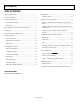
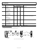
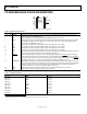
FUNCTIONAL BLOCK DIAGRAM
V
IN
1
10-/12-BIT
SUCCESSIVE
APPROXIMATION
ADC
CONTROL
LOGIC
I/P
MUX
AD7993/AD7994
V
DD
SCL
I
2
C INTERFACE
CYCLE TIMER
REGISTER
ALERT STATUS
REGISTER
CONFIGURATION
REGISTER
CONVERSION
RESULT
REGISTER
SDA
AGND
CONVST
AGND
AS
OSCILLATOR
REF
IN
V
IN
4
DATA
LOW
LIMIT
REGISTER CH1–CH4
T/H
DATA
HIGH
LIMIT
REGISTER CH1–CH4
HYSTERESIS
REGISTER CH1–CH4
03472-0-001
V
IN
2
V
IN
3
ALERT/
BUSY
Figure 1.
On-chip limit registers can be programmed with high and low
limits for the conversion result, and an open-drain, out-of-
range indicator output (ALERT) becomes active when the
programmed high or low limits are violated by the conversion
result. This output can be used as an interrupt.
PRODUCT HIGHLIGHTS
1. 2 µs conversion time with low power consumption.
2. I
2
C-compatible serial interface with pin-selectable
addresses. Two AD7993/AD7994 versions allow five
AD7993/AD7994 devices to be connected to the same
serial bus.
3. The parts feature automatic shutdown while not converting
to maximize power efficiency. Current consumption is
1 µA max when in shutdown mode.
4. Reference can be driven up to the power supply.
5. Out-of-range indicator that can be software disabled or
enabled.
6. One-shot and automatic conversion rates.
7. Registers can store minimum and maximum conversion
results.