
Datasheet

AD7993/AD7994
Rev. 0 | Page 10 of 32
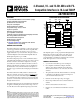
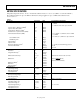
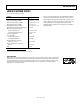
PIN CONFIGURATION AND PIN FUNCTION DESCRIPTIONS
AD7993/
AD7994
TOP VIEW
1
2
3
4
13
14
15
16
SDA
SCL
V
DD
A
GND
V
IN
4
10
9
V
IN
2
5
(Not to Scale)
ALERT/BUSY
12
11
AS
AGND
REF
IN
6
V
IN
1
7
V
IN
3
8
A
GND
A
GND
03472-0-003
CONVST
A
GND
Figure 3. 16-Lead TSSOP Pin Configuration
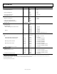
Table 5. Pin Function Descriptions
Pin No. Mnemonic Function
1, 2, 3, 4, 16 AGND
Analog Ground. Ground reference point for all circuitry on the AD7993/AD7994. All analog input signals
should be referred to this AGND voltage.
5 V
DD
Power Supply Input. The V
DD
range for the AD7993/AD7994 is from 2.7 V to 5.5 V.
6 REF
IN
Voltage Reference Input. The external reference for the AD7993/AD7994 should be applied to this input pin.
The voltage range for the external reference is 1.2 V to V
DD
. A 0.1 µF and 1 µF capacitor should be placed
between REF
IN
and AGND. See Figure 22.
7 V
IN
1 Analog Input 1. Single-ended analog input channel. The input range is 0 V to REF
IN
.
8 V
IN
3 Analog Input 3. Single-ended analog input channel. The input range is 0 V to REF
IN
.
9 V
IN
4 Analog Input 4. Single-ended analog input channel. The input range is 0 V to REF
IN
.
10 V
IN
2 Analog Input 2. Single-ended analog input channel. The input range is 0 V to REF
IN
.
11 AS
Logic Input. Address select input that selects one of three I
2
C addresses for the AD7993/AD7994, as shown in
Table 6. The device address depends on the voltage applied to this pin.
12
CONVST Logic Input Signal/Convert Start Signal. This is an edge-triggered logic input. The rising edge of this signal
powers up the part. The power-up time for the part is 1 µs. The falling edge of
CONVST places the track/hold
into hold mode and initiates a conversion. A power-up time of at least 1 µs must be allowed for the
CONVST
high pulse; otherwise, the conversion result is invalid (see the Modes of Operation section).
13 ALERT/BUSY
Digital Output, Selectable as an ALERT or BUSY Output Function. When configured as an ALERT, this pin acts
as an out-of-range indicator and, if enabled, becomes active when the conversion result violates the DATA
HIGH
or DATA
LOW
register values. See the Limit Registers section. When configured as a BUSY output, this pin
becomes active when a conversion is in progress. Open-drain output.
14 SDA Digital I/O. Serial bus bidirectional data. Open-drain output. External pull-up resistor required.
15 SCL Digital Input. Serial bus clock. External pull-up resistor required.
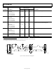
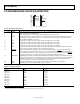
Table 6. I
2
C Address Selection
Part Number AS Pin I
2
C Address
AD7993-0 GND 010 0001
AD7993-0 V
DD
010 0010
AD7993-1 GND 010 0011
AD7993-1 V
DD
010 0100
AD7993-x
1
Float 010 0000
AD7994-0 GND 010 0001
AD7994-0 V
DD
010 0010
AD7994-1 GND 010 0011
AD7994-1 V
DD
010 0100
AD7994-x
1
Float 010 0000
1
If the AS pin is left floating on any of the AD7993/AD7994 parts, the device address is 010 0000.