
Datasheet
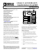

AD7993/AD7994
Rev. 0 | Page 2 of 32
TABLE OF CONTENTS
AD7993 Specifications..................................................................... 3
AD7994 Specifications..................................................................... 5
I
2
C Timing Specifications................................................................ 7
Absolute Maximum Ratings............................................................ 9
ESD Caution.................................................................................. 9
Pin Configuration and Pin Function Descriptions.................... 10
Ter mi nolog y .................................................................................... 11
Typical Performance Characteristics ........................................... 12
Circuit Information........................................................................ 15
Converter Operation.................................................................. 15
Typical Connection Diagram ................................................... 16
Analog Input ............................................................................... 16
Internal Register Structure ............................................................ 18
Address Pointer Register ........................................................... 18
Configuration Register .............................................................. 19
Conversion Result Register ....................................................... 20
Limit Registers ............................................................................ 20
Alert Status Register................................................................... 21
Cycle Timer Register.................................................................. 22
Sample Delay and Bit Trial Delay............................................. 22
Serial Interface ................................................................................ 23
Serial Bus Address...................................................................... 23
Writing to the AD7993/AD7994.................................................. 24
Writing to the Address Pointer Register for a Subsequent
Read
.............................................................................................. 24
Writing a Single Byte of Data to the Alert Status Register or
Cycle Register
.............................................................................. 24
Writing Two Bytes of Data to a Limit or Hysteresis
Register
........................................................................................ 24
Reading Data from the AD7993/AD7994................................... 26
Alert/Busy Pin................................................................................. 27
SMBus Alert ................................................................................ 27
Busy .............................................................................................. 27
Placing the AD7993-1/AD7994-1 into High Speed Mode... 27
The Address Select (AS) Pin ..................................................... 27
Modes of Operation ....................................................................... 28
Mode 1—Using the
CONVST
Pin ........................................... 28
Mode 2—Command Mode....................................................... 29
Mode 3—Automatic Cycle Interval Mode.............................. 30
Outline Dimensions ....................................................................... 31
Ordering Guide .......................................................................... 31
Related Parts in I
2
C-Compatible ADC Product Family........ 31
REVISION HISTORY
10/04—Revision 0: Initial Version