
Datasheet
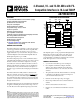

AD7993/AD7994
Rev. 0 | Page 3 of 32
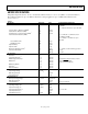
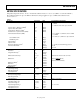
AD7993 SPECIFICATIONS
Temperature range for B version is −40°C to +125°C. Unless otherwise noted, V
DD
= 2.7 V to 5.5 V; REF
IN
= 2.5 V; For the AD7993-0,
all specifications apply for f
SCL
up to 400 kHz. For the AD7993-1, all specs apply for f
SCL
up to 3.4 MHz, unless otherwise noted.
T
A
= T
MIN
to T
MAX.
Table 1.
Parameter B Version Unit Test Conditions/Comments
DYNAMIC PERFORMANCE
1
F
IN
= 10 kHz sine wave for f
SCL
from
1.7 MHz
to 3.4 MHz
F
IN
= 1 kHz sine wave for f
SCL
up to 400 kHz
Signal-to-Noise + Distortion (SINAD)
2
61 dB min
Total Harmonic Distortion (THD)
2
–75 dB max
Peak Harmonic or Spurious Noise (SFDR)
2
–76 dB max
Intermodulation Distortion (IMD)
2
fa = 10.1 kHz, fb = 9.9 kHz for f
SCL
from
1.7 MHz to 3.4 MHz
fa = 1.1 kHz, fb = 0.9 kHz for f
SCL
up to
400 kHz
Second-Order Terms –86 dB typ
Third-Order Terms –86 dB typ
Aperture Delay
2
10 ns max
Aperture Jitter
2
50 ps typ
Channel-to-Channel Isolation
2
-90 dB typ F
IN
= 108 Hz, see the Terminology section
Full-Power Bandwidth
2
11 MHz typ @ 3 dB
2 MHz typ @ 0.1 dB
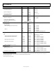
DC ACCURACY
Resolution 10 Bits
Integral Nonlinearity
1, 2
±0.5 LSB max
Differential Nonlinearity
1, 2
±0.5 LSB max Guaranteed no missed codes to 10 bits
Offset Error
2
±1.5 LSB max
Mode 1 (
CONVST Mode)
±2.5 LSB max Mode 2 (Command Mode)
Offset Error Match
2
±0.5 LSB max
Gain Error
2
±1.5 LSB max
Gain Error Match
2
±0.5 LSB max
ANALOG INPUT
Input Voltage Range 0 to REF
IN
V
DC Leakage Current ±1 µA max
Input Capacitance 30 pF typ
REFERENCE INPUT
REF
IN
Input Voltage Range 1.2 to V
DD
V min/V max
DC Leakage Current ±1 µA max
Input Impedance 69 kΩ typ During a conversion
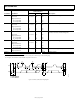
LOGIC INPUTS (SDA, SCL)
Input High Voltage, V
INH
0.7 (V
DD
) V min
Input Low Voltage, V
INL
0.3 (V
DD
) V max
Input Leakage Current, I
IN
±1 µA max V
IN
= 0 V or V
DD
Input Capacitance, C
IN
3
10 pF max
Input Hysteresis, V
HYST
0.1(V
DD
) V min