
Datasheet
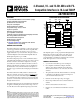

AD7993/AD7994
Rev. 0 | Page 8 of 32
AD7993/AD7994
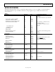
Limit at T
MIN
, T
MAX
Parameter Conditions Min Max Unit Description
t
10
Standard mode 300 ns t
FDA
, fall time of SDA signal
Fast mode 20 + 0.1 C
B
300 ns
High speed mode
C
B
= 100 pF max 10 80 ns
C
B
= 400 pF max 20 160 ns
t
11
Standard mode 1000 ns t
RCL
, rise time of SCL signal
Fast mode 20 + 0.1 C
B
300 ns
High speed mode
C
B
= 100 pF max 10 40 ns
C
B
= 400 pF max 20 80 ns
t
11A
Standard mode 1000 ns
t
RCL1
, rise time of SCL signal after a repeated start
condition and after an acknowledge bit
Fast mode 20 + 0.1 C
B
300 ns
High speed mode
C
B
= 100 pF max 10 80 ns
C
B
= 400 pF max 20 160 ns
t
12
Standard mode 300 ns t
FCL
, fall time of SCL signal
Fast mode 20 + 0.1 C
B
300 ns
High speed mode
C
B
= 100 pF max 10 40 ns
C
B
= 400 pF max 20 80 ns
t
SP
2
Fast mode 0 50 ns Pulse width of suppressed spike
High speed mode 0 10 ns
t
POWER-UP
1 typ µs Power-up time
1
A device must provide a data hold time for SDA in order to bridge the undefined region of the SCL falling edge.
2
For 3 V supplies, the maximum hold time with C
B
= 100 pF max is 100 ns max.
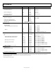
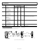
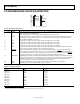
P
S
S
P
t
6
t
4
t
1
t
3
t
5
t
8
t
2
t
11
t
12
t
6
SCL
SDA
t
7
t
9
t
10
S = START CONDITION
P = STOP CONDITION
03472-0-002
Figure 2. Two-Wire Serial Interface Timing Diagram