
Datasheet


AD8112
Rev. 0 | Page 7 of 28
ABSOLUTE MAXIMUM RATINGS
Table 6.
Parameter Rating
Analog Supply Voltage (AV
CC
to AV
EE
) 26.0 V
Digital Supply Voltage (DV
CC
to DGND) 6 V
Ground Potential Difference (AGND to DGND) ±0.5 V
Internal Power Dissipation
1
3.1 W
Analog Input Voltage
2
Maintain linear output
Digital Input Voltage DV
CC
Output Voltage (Disabled Output) (AV
CC
− 1.5 V) to
(AV
EE
+ 1.5 V)
Output Short-Circuit Duration Momentary
Storage Temperature Range −65°C to +125°C
Lead Temperature (Soldering 10 sec) 300°C
1
Specification is for device in free air (T
A
= 25°C):
100-lead plastic LQFP (ST): θ
JA
= 40°C/W.
2
To avoid differential input breakdown, ensure that one-half the output
voltage (1/2 V
OUT
) and any input voltage is less than 10 V of the potential
differential. See Output Voltage Swing specification for linear output range.
Stresses above those listed under Absolute Maximum Ratings
may cause permanent damage to the device. This is a stress
rating only; functional operation of the device at these or any
other conditions above those indicated in the operational
section of this specification is not implied. Exposure to absolute
maximum rating conditions for extended periods may affect
device reliability.
ESD CAUTION
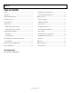
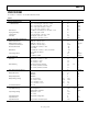
POWER DISSIPATION
The AD8112 is operated with ±5 V to ±12 V supplies and can
drive loads down to 150 Ω (±5 V) or 600 Ω (±12 V), resulting
in a large range of possible power dissipations. For this reason,
extra care must be taken when derating the operating conditions
based on ambient temperature.
Packaged in a 100-lead LQFP, the AD8112 junction-to-ambient
thermal impedance (θ
JA
) is 40°C/W. For long-term reliability,
the maximum allowed junction temperature of the plastic encap-
sulated die should not exceed 150°C. Temporarily exceeding
this limit may cause a shift in parametric performance due
to a change in the stresses exerted on the die by the package.
Exceeding a junction temperature of 175°C for an extended
period can result in device failure. The curve in
Figure 4 shows
the range of allowed power dissipations that meet these conditions
over the commercial range of ambient temperatures.
4.0
MAXIMUM POWER (W)
3.5
2.0
3.0
2.5
AMBIENT TEMPERATURE (°C)
0 1020304050607
0
T
J
= 150°C
06523-004
Figure 4. Maximum Power Dissipation vs. Ambient Temperature