
Datasheet


Table Of Contents
Evaluation Board User Guide
UG-130
One Technology Way • P. O. Box 9106 • Norwood, MA 02062-9106, U.S.A. • Te l: 781.329.4700 • Fax: 781.461.3113 • www.analog.com
Differential Amplifier Evaluation Board for 8-lead SOIC and MSOP Packages
PLEASE SEE THE LAST PAGE FOR AN IMPORTANT
WARNING AND LEGAL TERMS AND CONDITIONS.
Rev. B | Page 1 of 8
FEATURES
Flexible board layout
Accommodates AD8131/AD8132/AD8138/AD8139
Accommodates various circuit configurations
Enables quick breadboarding/prototyping
Edge-mounted circuit configuration
Easy connection to test equipment and other circuits
RoHS compliant
GENERAL DESCRIPTION
An Analog Devices, Inc., differential driver evaluation board
makes it easy for designers to obtain quick performance results
for their particular differential driver application circuits. The
board layout is very flexible and allows for many circuit configura-
tions, including traditional four-resistor circuits, circuits with
two different feedback loops, circuits with input and output
transformers, filters, and many others. Most resistors and
capacitors use 1206 packages.
The board accommodates the AD8131, AD8132, AD8138, and
AD8139. The data sheets for these devices should be consulted
in conjunction with this evaluation board user guide.
The AD8131 is a special case because it has internal feedback
networks but can, nonetheless, be evaluated on the board by
• Omitting the R19 and R20 feedback resistors and C3 and
C4 capacitors.
• Using 0 Ω resistors for Gain Resistor R17 and Gain
Resistor R18.
• Ignoring all further references to these components.
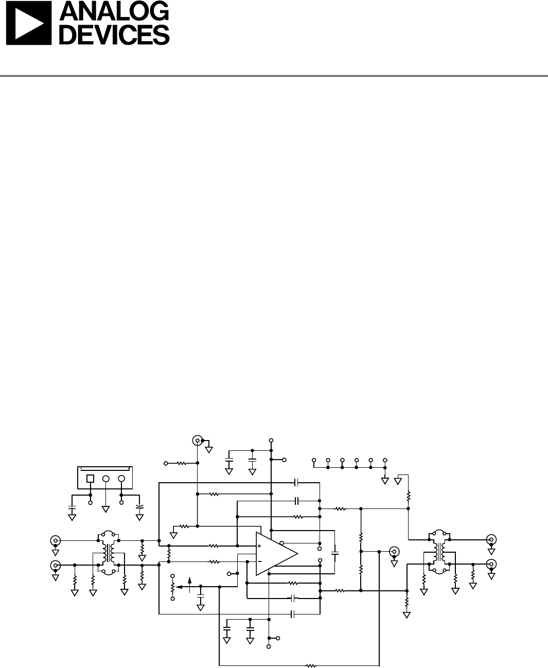
DIFFERENTIAL DRIVER EVALUATION BOARD SCHEMATIC
J3
J4
R4
R2
R3
JP1
P1
1
2
V+ V–
C2
+
+
C1
R6
R7
JP2
T1, T3
3
R5
R18
R17
R1
V–
V+
C9
CW
TP4
2
1
8
V
OCM
DUT
C10
C11
TP3
V–
C6
C4
R20
6
4
5
3
TP1
R19
C3
C5
J1
J2
R10
R9
JP4
R8
JP3
T2, T4
C13
R15
R16
V+
C12
C8
TP2
R12
R11
PR1
R21
R13
R14
08988-001
TP10TP5 TP6 TP7 TP8 TP9
7
R23
R24
R22
J5
V–
Figure 1. Evaluation Board Schematic