
Datasheet


6.25 Gbps, 4 × 4,
Digital Crosspoint Switch with EQ
AD8156
Rev. 0
Information furnished by Analog Devices is believed to be accurate and reliable. However, no
responsibility is assumed by Analog Devices for its use, nor for any infringements of patents or other
rights of third parties that may result from its use. Specifications subject to change without notice. No
license is granted by implication or otherwise under any patent or patent rights of Analog Devices.
Trademarks and registered trademarks are the property of their respective owners.
One Technology Way, P.O. Box 9106, Norwood, MA 02062-9106, U.S.A.
Tel: 781.329.4700 www.analog.com
Fax: 781.461.3113 ©2007 Analog Devices, Inc. All rights reserved.
FEATURES
4 × 4, fully differential, nonblocking array
Configurable for dual 2 × 2 operation
DC to 6.25 Gbps per channel, NRZ data rate
Programmable input equalization compensates for over 40”
of FR-4 at 6.25 Gbps
Multicast and broadcast modes of operation
Programmable output swing
100 mV p-p to 1.6 V p-p differential
Power supply: 3.3 V (±10%)
Low power
No EQ: 400 mW typical
Maximum EQ: 700 mW typical
Inputs: ac-coupled or dc-coupled
Wide set of dc-coupled input standards
3.3 V/2.5 V/1.8 V CML or 3.3 V LVPECL
Control: LVTTL- or LVCMOS-compatible
Low additive jitter: 25 ps p-p typical
Low random jitter: 0.8 ps rms
Integrated 50 Ω termination impedance at inputs/outputs
Individual output disable for power savings
49-ball, 8 mm × 8 mm BGA, 1 mm pitch
APPLICATIONS
Backplane equalization
SONET/SDH
Gigabit Ethernet
XAUI
Fibre Channel
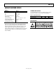
FUNCTIONAL BLOCK DIAGRAM
EQ
4
4
CS
RST
UPD
WE
RE
MODE
D[3:0]
A[3:0]
CONTROL
LOGIC
AD8156
IN0P/N
IN1P/N
IN2P/N
IN3P/N
OUT0P/N
OUT1P/N
OUT2P/N
OUT3P/N
EQ
EQ
EQ
OUTPUT
DRIVERS
INPUT
RECEIVERS
INPUT
EQUALIZATION
4 × 4
SWITCH
06305-001
Figure 1.
GENERAL DESCRIPTION
The AD8156, a member of the Xstream line of products, is a
high speed, fully differential, digital crosspoint switch. The part
can function as a 4 × 4 crosspoint switch with double-latched
memory, allowing simultaneous updates, or as a dual 2 × 2 with
direct output control. The AD8156 has low power dissipation,
typically 700 mW on 3.3 V with all outputs and input equalizers
active. It operates at any data rate from dc to 6.25 Gbps per port.
Each input channel on the AD8156 has a programmable input
equalizer to compensate for signal loss over a backplane.
The AD8156 high speed inputs are compatible with both ac-
coupled and dc-coupled 3.3 V, 2.5 V, or 1.8 V CML, as well as
3.3 V LVPECL data levels. The control interface is LVTTL- and
LVCMOS-compatible at 3.3 V. All input and output termination
resistors are integrated for ease of layout and to minimize
impedance mismatch. Input equalization and unused outputs
can be individually disabled to minimize power dissipation.
The AD8156 is packaged in a 49-ball, 8 mm × 8 mm, BGA
package with a 1 mm ball pitch. It operates over the industrial
temperature range of −40°C to 85°C.