
Datasheet
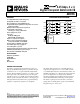


AD8156
Rev. 0 | Page 8 of 20
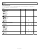
PIN CONFIGURATIONS AND FUNCTION DESCRIPTIONS
A
B
C
D
E
F
G
7654321
06305-007
V
EE
IN1NIN1PV
TTI
IN0NIN0PV
CC
IN2PV
EE
D3V
EE
MODEV
CC
OUT0P
IN2ND0D2RSTWECSOUT0N
V
TTI
V
EE
D1V
EE
UPDV
CC
V
TTO
IN3PA0A1A3REV
CC
OUT1P
IN3NV
CC
A2V
EE
V
EE
V
EE
OUT1N
V
CC
OUT3NOUT3PV
TTO
OUT2NOUT2PV
EE
Figure 7. Pin Configuration (Bottom View)
Table 5. Pin Function Descriptions
Pin No. Mnemonic Description
A1 V
EE
Negative Supply.
A2 IN1N High Speed Input Complement.
A3 IN1P High Speed Input.
A4 V
TTI
Input Termination Supply.
A5 IN0N High Speed Input Complement.
A6 IN0P High Speed Input.
A7 V
CC
Positive Supply.
B1 IN2P High Speed Input.
B2 V
EE
Negative Supply.
B3 D3 Input Address Pin (MSB).
B4 V
EE
Negative Supply.
B5 MODE Mode Select Pin.
B6 V
CC
Positive Supply.
B7 OUT0P High Speed Output.
C1 IN2N High Speed Input Complement.
C2 D0 Input Address Pin (LSB).
C3 D2 Input Address Pin.
C4
RST
Reset/Disable Outputs.
C5
WE
First Bank Write Enable.
C6
CS
Chip Select Enable.
C7 OUT0N High Speed Output Complement.
D1 V
TTI
Input Termination Supply.
D2 V
EE
Negative Supply.
D3 D1 Input Address Pin.
D4 V
EE
Negative Supply.
Pin No. Mnemonic Description
D5
UPD
Second Bank Write Enable.
D6 V
CC
Positive Supply.
D7 V
TTO
Output Termination Supply.
E1 IN3P High Speed Input.
E2 A0 Address Pin (LSB).
E3 A1 Address Pin.
E4 A3 Address Pin (MSB).
E5
RE
Second Bank Read Enable.
E6 V
CC
Positive Supply.
E7 OUT1P High Speed Output.
F1 IN3N High Speed Input Complement.
F2 V
CC
Positive Supply.
F3 A2 Address Pin.
F4 V
EE
Negative Supply.
F5 V
EE
Negative Supply.
F6 V
EE
Negative Supply.
F7 OUT1N High Speed Output Complement.
G1 V
CC
Positive Supply.
G2 OUT3N High Speed Output Complement.
G3 OUT3P High Speed Output.
G4 V
TTO
Output Termination Supply.
G5 OUT2N High Speed Output Complement.
G6 OUT2P High Speed Output.
G7 V
EE
Negative Supply.