
Datasheet


Table Of Contents
AD8225 Evaluation Board
AD8225-EVALZ
Rev. A
Evaluation boards are only intended for device evaluation and not for production purposes.
Evaluation boards are supplied “as is” and without warranties of any kind, express, implied, or
statutory including, but not limited to, any implied warranty of merchantability or fitness for a
particular purpose. No license is granted by implication or otherwise under any patents or other
intellectual property by application or use of evaluation boards. Information furnished by Analog
Devices is believed to be accurate and reliable. However, no responsibility is assumed by Analog
Devices for its use, nor for any infringements of patents or other rights of third parties that may result
from its use. Analog Devices reserves the right to change devices or specifications at any time
without notice. Trademarks and registered trademarks are the property of their respective owners.
Evaluation boards are not authorized to be used in life support devices or systems.
One Technology Way, P.O. Box 9106, Norwood, MA 02062-9106, U.S.A.
Tel: 781.329.4700 www.analog.com
Fax: 781.461.3113 ©2003–2007 Analog Devices, Inc. All rights reserved.
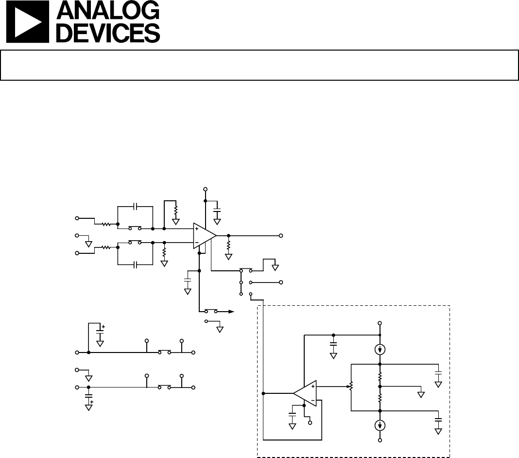
BOARD DESCRIPTION
The AD8225 evaluation board has been carefully laid out and
tested to demonstrate the performance of the device.
Figure 1 is
a schematic of an evaluation board available for the AD8225.
The board is shipped with an AD8225 already installed. The
user need only connect power and an input to conduct
measurements. The supply can be configured for dual or single
supplies, and the input can be dc- or ac-coupled. A circuit is
provided on the board so the user can zero the output offset. If
desired, a reference can be applied from an external voltage source.
NOTES
REMOVE W3 AND W4 FOR AC COUPLING
*INSTALL FOR AC COUPLIN
G
A1
2
3
W3
W4
C1
0.1µF
C3
0.1µF
C10
0.1µF
C8
0.1µF
C7
0.1µF
R2
100Ω
R4
100Ω
R5
100kΩ*
R3
100kΩ*
+IN
GND
–IN
+
V
S
OUTPUT
R8
5
4
1
C2
0.1µF
C12
10µF, 25V
C11
10µF, 25V
W12
EXT_REF
W13
W11
W14
–V
S
+V
S
GND
–V
S
W7
W6
+V
AUX
–V
AUX
–V
AUX
–V
AUX
+V
AUX
C9
0.1µF
4
6
7
3
2
A1
OFFSET
ADJ
CS3
J500
240µA
CS1
J500
240µA
OP177
USER-SUPPLIED
7
6
C4
0.1µF
R10
5.9kΩ, 1%
R9
5.9kΩ, 1%
R1
10kΩ
03596-001
Figure 1. Evaluation Board Schematic