
Datasheet


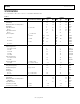

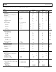


Table Of Contents

Data Sheet AD822
Rev. J | Page 9 of 24
Parameter Test Conditions/Comments
A Grade B Grade
Unit Min Typ Max Min Typ Max
OUTPUT CHARACTERISTICS
Output Saturation Voltage
2
V
OL
− V
EE
I
SINK
= 20 µA 5 7 5 7 mV
T
MIN
to T
MAX
10 10 mV
V
CC
− V
OH
I
SOURCE
= 20 µA 10 14 10 14 mV
T
MIN
to T
MAX
20 20 mV
V
OL
− V
EE
I
SINK
= 2 mA 40 55 40 55 mV
T
MIN
to T
MAX
80 80 mV
V
CC
− V
OH
I
SOURCE
= 2 mA 80 110 80 110 mV
T
MIN
to T
MAX
160 160 mV
V
OL
− V
EE
I
SINK
= 15 mA 300 500 300 500 mV
T
MIN
to T
MAX
1000
1000
mV
V
CC
− V
OH
I
SOURCE
= 15 mA 800 1500 800 1500 mV
T
MIN
to T
MAX
1900 1900 mV
Operating Output Current 20 20 mA
T
MIN
to T
MAX
15 15 mA
Capacitive Load Drive 350 350 pF
POWER SUPPLY
Quiescent Current, T
MIN
to T
MAX
1.4 1.8 1.4 1.8 mA
Power Supply Rejection V
SY
= ±5 V to ±15 V 70 80 70 80 dB
T
MIN
to T
MAX
70 70 dB
1
This is a functional specification. Amplifier bandwidth decreases when the input common-mode voltage is driven in the range (V+ − 1 V) to V+. Common-mode error
voltage is typically less than 5 mV with the common-mode voltage set at 1 V below the positive supply.
2
V
OL
− V
EE
is defined as the difference between the lowest possible output voltage (V
OL
) and the negative voltage supply rail (V
EE
). V
CC
− V
OH
is defined as the difference
between the highest possible output voltage (V
OH
) and the positive supply voltage (V
CC
).