Evaluation Board User Guide UG-003 One Technology Way • P.O. Box 9106 • Norwood, MA 02062-9106, U.S.A. • Tel: 781.329.4700 • Fax: 781.461.3113 • www.analog.
UG-003 Evaluation Board User Guide TABLE OF CONTENTS Features .............................................................................................. 1 Input Signals...................................................................................3 Equipment Needed ........................................................................... 1 Output Signals ...............................................................................3 Software Needed .........................................
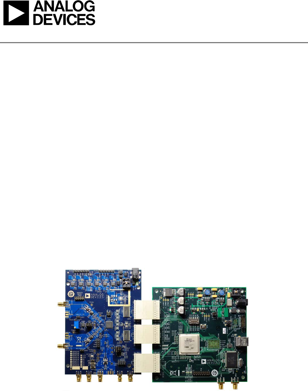
Evaluation Board User Guide UG-003 EVALUATION BOARD HARDWARE The evaluation board provides all of the support circuitry required to operate these parts in their various modes and configurations. Figure 2 shows the typical bench characterization setup used to evaluate the ac performance. It is critical that the signal sources used for the analog input and clock have very low phase noise (<1 ps rms jitter) to realize the optimum performance of the signal chain.
UG-003 Evaluation Board User Guide WALL OUTLET 100V ac TO 240V ac 47Hz TO 63Hz SWITCHING POWER SUPPLY SWITCHING POWER SUPPLY 6V dc 2A MAX SIGNAL GENERATOR 6V dc 2A MAX ANALOG FILTER SIGNAL GENERATOR ANALOG FILTER PC RUNNING VISUAL ANALOG AND SPI CONTROLLER USER SOFTWARE CLOCK SOURCE Figure 2. Evaluation Board Connection Rev.
Evaluation Board User Guide UG-003 15pF 0.1µF 0.1µF VCM 2V p-p 33Ω 0Ω 0.1µF 15Ω VIN+ 33Ω 2.2pF AD9650 5pF 33Ω 15Ω VIN– 08168-003 33Ω 0.1µF 15pF Figure 3. Default Analog Input Configuration of the AD9650 Family FERRITE BEAD 10Ω @ 100MHz 0.1µF VCM 2V p-p 0Ω 0.1µF 66.5Ω 33Ω VIN+ AD9268/ AD9258 33Ω 66.5Ω VIN– FERRITE BEAD 10Ω @ 100MHz 0.1µF 08168-031 0.1µF Figure 4. Default Analog Input Configuration of the AD9268 Family 0.1µF VCM 2V p-p 0.1µF 33Ω 0Ω 0.
UG-003 Evaluation Board User Guide VREF Clock Circuitry for the AD9650 and the AD9268 Family The default VREF configuration is to connect the SENSE pin to AGND for internal VREF operation. This is done by connecting Pin 4 and Pin 6 on Header J201. Table 2 summarizes the internal VREF voltage for the different families of ADCs.
Evaluation Board User Guide UG-003 Switching Power Supply Optionally, the ADC on the board can be configured to use the ADP2114 dual switching power supply to provide power to the DRVDD and AVDD rails of the ADC. To configure the board to operate from the ADP2114, the following changes must be incorporated (see the Evaluation Board Schematics and Artwork and Bill of Materials sections for specific recommendations for part values): 1. 2. 3. 4. 5. 6. 7. 8. Install L101, L102, E116, and E117.
UG-003 Evaluation Board User Guide EVALUATION BOARD SOFTWARE QUICK START PROCEDURES This section provides quick start procedures for using the AD9650, AD9268, AD9258, AD9251, AD9231, AD9204, AD9269, and AD6659 evaluation board. Both the default and optional settings are described. CONFIGURING THE BOARD 2. 3. 4. 5. 6. 7. Connect the evaluation board to the data capture board, as shown in Figure 1 and Figure 2. Connect one 6 V, 2.5 A switching power supply (such as the CUI, Inc.
UG-003 08168-008 Evaluation Board User Guide Figure 9. VisualAnalog, Main Window Setting Up the SPI Controller Software Open the SPI controller software by going to the Start menu or by double-clicking the SPIController software desktop icon. If prompted for a configuration file, select the appropriate one. If not, check the title bar of the window to determine which configuration is loaded. If necessary, choose Cfg Open from the File menu and select the appropriate file based on your part type.
UG-003 Note that other settings can be changed on the ADCBase 0 page (see Figure 12) and the ADC A and ADC B pages (see Figure 13) to set up the part in the desired mode. The ADCBase 0 page settings affect the entire part, whereas the settings on the ADC A and ADC B pages affect the selected channel only.
Evaluation Board User Guide UG-003 Troubleshooting Tips If the FFT plot appears abnormal, do the following: If the FFT window remains blank after Run is clicked, do the following: • • • If you see a normal noise floor when you disconnect the signal generator from the analog input, be sure you are not overdriving the ADC. Reduce the input level, if necessary. In VisualAnalog, click the Settings button in the Input Formatter block.
UG-003 Evaluation Board User Guide EVALUATION BOARD SCHEMATICS AND ARTWORK 08168-016 Figure 17. Board Power Input and Supply Circuits Rev.
Evaluation Board User Guide UG-003 08168-017 Figure 18. DUT and Related Circuits Rev.
UG-003 Evaluation Board User Guide 08168-018 Figure 19. SPI Interface Circuit Rev.
Evaluation Board User Guide UG-003 08168-019 Figure 20. Channel A Input Circuits Rev.
UG-003 Evaluation Board User Guide 08168-020 Figure 21. Channel B Analog Input Circuits Rev.
Evaluation Board User Guide UG-003 08168-021 Figure 22. Default Clock Path Input Circuits Rev.
UG-003 Evaluation Board User Guide 08168-022 Figure 23. Optional AD9517 Clock Input Circuit Rev.
Evaluation Board User Guide UG-003 08168-023 Figure 24. Output Buffer Circuits Rev.
UG-003 Evaluation Board User Guide 08168-024 Figure 25. FIFO Board Connector Rev.
UG-003 08168-025 Evaluation Board User Guide Figure 26. Top Side Rev.
Evaluation Board User Guide 08168-026 UG-003 Figure 27. Ground Plane (Layer 2) Rev.
UG-003 08168-027 Evaluation Board User Guide Figure 28. Power Plane (Layer 3) Rev.
Evaluation Board User Guide 08168-028 UG-003 Figure 29. Power Plane (Layer 4) Rev.
UG-003 08168-029 Evaluation Board User Guide Figure 30. Ground Plane (Layer 5) Rev.
Evaluation Board User Guide 08168-030 UG-003 Figure 31. Bottom Side Rev.
Evaluation Board User Guide UG-003 ORDERING INFORMATION BILL OF MATERIALS Table 3.
UG-003 Evaluation Board User Guide Item 301 Qty 0 311 321 331 341 351 0 0 0 0 0 361 371 381 391 0 0 0 0 401 411 421 0 0 0 Reference Designator C501, R120, R122, R124, R125, R126, R127, R305, R306, R307, R308, R405, R407, R410, R411, R413, R414, R415, R423, R505, R507, R510, R511, R514, R515, R516, R517, R519, R520, R521, R603, R604, R605, R607, R608, R721, R722, R731, R732 R518 R201 R202 R204, R205 R401, R402, R501, R502, R601 R406, R506, R719, R720 R412 R416 R417, R418, R419, R420, R421 R512, R51
Evaluation Board User Guide Reference Designator C116, C118, C120, C122, C149, C150, C151, C152, C153, C154, C204, C206, C207, C208, C209, C211, C301, C302, C401, C404, C405, C406, C407, C417, C418, C420, C426, C503, C505, C506, C507, C515, C516, C523, R524, C601, C602, C603, C606, C607, C609, C701, C702, C710, C711, C712, C713, C714, C715, C716, C717, C718, C719, C720, C721, C723, C724, C730, C731, C801, C802, C803, C804, C805, C806, C807, C808, C809 C403, C504 Item 55 Qty 68 55A1 0 56 6 57 58A 3 2
UG-003 Evaluation Board User Guide Item 72 Qty 4 Reference Designator J203, J402, J501, J602 Description CONN-PCB Value SMA, ST edge mount 73 74 75 76 77 78 79 1 2 1 3 1 2 3 J205 J301, J701 J302 J403, J503, J605 J404 JP101, JP103 JP503, L402, L501 CONN-PCB header CONN-PCB header CONN-PCB header CONN-PCB header CONN-PCB header Resistor, 0805, SMD Resistor, 0603, SMD 4P double row 8-pin double row ST male, 9-pin 2 position, single row ST 10P 0.
Evaluation Board User Guide Item 103 Qty 9 104 5 105 3 Reference Designator RN801, RN802, RN803, RN804, RN805, RN806, RN807, RN808, RN809 T401, T402, T501, T502, T602 U101, U104, U105 106 2 U102, U106 107 1 U103 108 109 1 1 U201 U301 110 3 U302, U703, U803 111 112 1 1 U401 U501 113 1 U701 114 2 U801, U802 115 1 VR101 116 1 Y601 1 UG-003 Description Resistor array Value 22 Ω, 8 term, SMD Manufacturer/Part No.
UG-003 Evaluation Board User Guide Item 8 Qty 27 9 10 1 1 Reference Designator C401, C402, C502, JP403, R203, R301, R302, R303, R304, R424, R425, R524, R525, R526, R606, R609, R610, R611, R612, R708, R715, R723, R727, R728, R729, R803, R804 C604 C705 Description Res film, SMD, 0402 Value 0Ω Manufacturer/Part No. Panasonic/ERJ-2GE0R00X 1000 pF 1800 pF Panasonic/ECU-E1E102KBQ Panasonic/ECJ-0EB1E182K C706 Capacitor, ceramic Capacitor, ceramic, multilayer, X7R, 0402 Capacitor, ceramic 11 1 0.
Evaluation Board User Guide Item 39 40 Qty 2 8 Reference Designator R113, R115 R206, R208, R209, R309, R316, R317, R801, R802 R207, R733 41 2 42 13 43 5 R121, R123, R310, R311, R312, R422, R522, R614, R704, R705, R706, R707, R709 R105, R106, R313, R314, R315 44 46 5 4 1 R403, R404, R503, R504, R741 R408, R409, R508, R509 R602 47 1 R710 48 1 R711 49 8 50 51 2 2 R714, R716, R725, R730, R738, R739, R805, R806 R726, R740 R734, R736 52 2 R735, R737 53 9 54 5 RN801, RN802, RN803, RN
UG-003 Item 68 Qty 1 Evaluation Board User Guide Reference Designator Y601-80 for -80 model U201 69 1 C108, C109 701 C110 711 C111, C113, C519 721 731 741 761 C112 C137, C140 C408, C409, C410, C411, C508, C509, C510, C511 C201, C202, C412, C413, C414, C415, C416, C421, C427, C512, C513, C521, C522, C610, C703, C704, C708, C709 C422, C423 771 781 C424 C425 791 801 C517, C518 C520 811 821 E104, E106, E108, E116, E117, E118, E119 J401, J502, J601, J702, J703, J704 831 JP102, JP104 841 851 8
Evaluation Board User Guide Item 1031 Qty Reference Designator R401, R402, R501, R502, R601 1041 R406, R506, R719, R720 1051 R412 1061 1071 R416 R417, R418, R419, R420, R421 1081 R512, R513 1091 1101 1111 1121 R613 T403, T503 T404 T505 1131 1141 1161 T601 TP101, TP102, TP402, TP601, TP801, TP802 TP9, TP401, TP701, TP702, TP703, TP704, TP705 U702 1171 CR201 1181 U202 1151 1 UG-003 Description Res prec, thick film chip, R0603 Res prec, thick film chip, R0402 Res prec, thick film chip, R0
UG-003 Evaluation Board User Guide Item 9 10 Qty 2 1 Reference Designator C410, C510 C705 11 12 13 14 1 1 1 5 C706 C707 C722 CR101, CR102, CR104, CR105, CR106 15 1 CR103 16 1 CR601 17 18 3 12 19 1 CR701, CR801, CR802 E101, E102, E103, E105, E107, E109, E110, E111, E112, E113, E114, E115 F101 20 1 FL101 21 1 J201 22 4 J203, J402, J501, J602 23 1 J205 24 2 J301, J701 25 1 J302 26 3 J403, J503, J605 27 1 J404 28 2 JP101, JP103 29 30 7 1 JP503, L402, L403, L404, L
Evaluation Board User Guide Item 41 Qty 13 Reference Designator R121, R123, R310, R311, R312, R422, R522, R614, R704, R705, R706, R707, R709 R105, R106, R313, R314, R315 42 5 43 9 44 1 R403, R404, R408, R409, R503, R504, R508, R509, R741 R602 1 R710 46 1 R711 47 8 48 49 2 2 R714, R716, R725, R730, R738, R739, R805, R806 R726, R740 R734, R736 50 2 R735, R737 51 9 52 4 RN801, RN802, RN803, RN804, RN805, RN806, RN807, RN808, RN809 T401, T402, T501, T502, 53 54 1 3 T601 U101, U104,
UG-003 Item 68 Qty 1 Evaluation Board User Guide Reference Designator Y601-20 for -20 model U201 69 1 C108, C109 701 C110 711 C111, C113, C519 721 731 C112 C137, C140 741 751 761 C408, C409, C411, C508, C509, C511 C201, C202, C412, C413, C414, C415, C416, C421, C427, C512, C513, C521, C522, C601, C703, C704, C708, C709 C422, C423 771 781 C424 C425 791 801 C517, C518 C520 811 821 E104, E106, E108, E116, E117, E118, E119 J401, J502, J601, J702, J703, J704 831 JP102, JP104 841 851 861 871
Evaluation Board User Guide Item 1031 Qty Reference Designator R401, R402, R501, R502, R601 1041 R406, R506, R719, R720 1051 R412 1061 1071 R416 R417, R418, R419, R420, R421 1081 R512, R513 1091 1101 1111 1121 R613 T403, T503 T404 T505, T602 1131 1151 TP101, TP102, TP402, TP601, TP801, TP802 TP9, TP401, TP701, TP702, TP703, TP704, TP705 U702 1161 CR201 1171 U202 1141 1 UG-003 Description Res prec, thick film, chip, R0603 Res prec, thick film, chip, R0402 Res prec, thick film, chip, R04
UG-003 Evaluation Board User Guide NOTES ESD Caution ESD (electrostatic discharge) sensitive device. Charged devices and circuit boards can discharge without detection. Although this product features patented or proprietary protection circuitry, damage may occur on devices subjected to high energy ESD. Therefore, proper ESD precautions should be taken to avoid performance degradation or loss of functionality.