
Datasheet

Data Sheet AD9215
Rev. B | Page 3 of 36
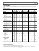
SPECIFICATIONS
AVDD = 3 V, DRVDD = 2.5 V, specified maximum conversion rate, 2 V p-p differential input, 1.0 V internal reference, unless otherwise
noted.
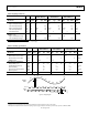
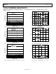
Table 1. DC Specifications
AD9215BRU-65/
AD9215BCP-65
AD9215BRU-80/
AD9215BCP-80
AD9215BRU-105/
AD9215BCP-105
Parameter
Temp
Test
Level
Min
Typ
Max
Min
Typ
Max
Min
Typ
Max
Unit
RESOLUTION Full VI 10 10 10 Bits
ACCURACY
No Missing Codes Full VI Guaranteed Guaranteed Guaranteed
Offset Error
1
Full VI ±0.3 ±2.0 ±0.3 ±2.0 ±0.3 ±2.0 % FSR
Gain Error
1
Full VI 0 +1.5 +4.0 +1.5 +4.0 +1.5 +4.0 % FSR
Differential Nonlinearity (DNL)
2
Full VI −1.0 ±0.5 +1.0 −1.0 ±0.5 +1.0 −1.0 ±0.6 +1.2 LSB
Integral Nonlinearity (INL)
2
Full VI ±0.5 ±1.2 ±0.5 ±1.2 ±0.65 ±1.2 LSB
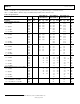
TEMPERATURE DRIFT
Offset Error
1
Full V +15 +15 +15 ppm/°C
Gain Error
1
Full V +30 +30 +30 ppm/°C
Reference Voltage (1 V Mode) Full V ±230 ±230 ±230 ppm/°C
INTERNAL VOLTAGE REFERENCE
Output Voltage Error (1 V Mode) Full VI ±2 ±35 ±2 ±35 ±2 ±35 mV
Load Regulation @ 1.0 mA Full V 0.2 0.2 0.2 mV
Output Voltage Error (0.5 V Mode) Full V ± 1 ±1 ±1 mV
Load Regulation @ 0.5 mA Full V 0.2 0.2 0.2 mV
INPUT REFERRED NOISE
VREF = 0.5 V 25°C V 0.8 0.8 0.8 LSB rms
VREF = 1.0 V 25°C V 0.4 0.4 0.4 LSB rms
ANALOG INPUT
Input Span, VREF = 0.5 V Full IV 1 1 1 V p-p
Input Span, VREF = 1.0 V Full IV 2 2 2 V p-p
Input Capacitance
3
Full V 2 2 2 pF
REFERENCE INPUT RESISTANCE Full V 7 7 7 kΩ
POWER SUPPLIES
Supply Voltage
AVDD Full IV 2.7 3.0 3.3 2.7 3.0 3.3 2.7 3.0 3.3 V
DRVDD Full IV 2.25 2.5 3.6 2.25 2.5 3.6 2.25 2.5 3.6 V
Supply Current
I
AVDD
2
Full VI 32 35 34.5 39 40 44 mA
I
DRVDD
2
25°C V 7.0 8.6 11.3 mA
PSRR Full V ± 0.1 ± 0.1 ± 0.1 % FSR
POWER CONSUMPTION
Sine Wave Input
2
I
AVDD
2
Full VI 96 104 120 mW
I
DRVDD
2
25°C V 18 20 25 mW
Standby Power
4
25°C V 1.0 1.0 1.0 mW
1
With a 1.0 V internal reference.
2
Measured at f
IN
= 2.4 MHz, full-scale sine wave, with approximately 5 pF loading on each output bit.
3
Input capacitance refers to the effective capacitance between one differential input pin and AGND. Refer to Figure 5 for the equivalent analog input structure.
4
Standby power is measured with a dc input, the CLK pin inactive (i.e., set to AVDD or AGND).