
Datasheet

Data Sheet AD9215
Rev. B | Page 7 of 36
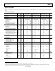
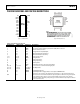
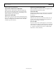
PIN CONFIGURATIONS AND FUNCTION DESCRIPTIONS
02874-A-003
1
2
3
4
5
6
7
8
9
10
11
12
13
14
OR
MODE
SENSE
VREF
REFB
REFT
AVDD
AGND
VIN+
VIN–
AGND
AVDD
CLK
PDWN
D9 (MSB)
D8
D7
D6
DRVDD
DRGND
D5
D4
D3
D2
D1
D0 (LSB)
DNC
28
27
26
25
24
23
22
21
20
19
18
17
16
15
AD9215
TOP VIEW
(Not to Scale)
DNC = DO NOT CONNECT
DNC
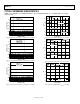
Figure 3. TSSOP (RU-28)
0
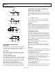
2874-A-004
19
17
20
21
18
14
13
12
11
10
9
15
16
D5
D
4
D3
D2
D1
(LSB) D0
DRGND
DRVDD
32
31
30
29
28
27
26
25
A
VDD
AGN
D
VIN–
VIN+
AGN
D
AVDD
REFT
REFB
22
23
24
D8
D6
D9 (MSB)
OR
D7
MODE
SENSE
VREF
1
2
3
4
5
6
7
8
DNC
CLK
DNC
PDWN
DNC
DNC
DNC
DNC
AD9215
TOP VIEW
(Not to Scale)
NOTES
1. DNC = DO NOT CONNECT.
2. IT IS RECOMMENDED THAT THE EXPOSED PAD BE SOLDERED
TO THE GROUND PLANE FOR THE LFCSP PACKAGE. THERE IS
AN INCREASED RELIABILITY OF THE SOLDER JOINTS, AND
THE MAXIMUM THERMAL CAPABILITY OF THE PACKAGE IS
ACHIEVED WITH THE EXPOSED PAD SOLDERED TO THE
CUSTOMER BOARD.
Figure 4. LFCSP (CP-32-7)
Table 6. Pin Function Descriptions
TSSOP Pin No. LFCSP Pin No. Mnemonic Description
1 21 OR Out-of-Range Indicator.
2 22 MODE Data Format and Clock Duty Cycle Stabilizer (DCS) Mode Selection.
3 23 SENSE Reference Mode Selection.
4 24 VREF Voltage Reference Input/Output.
5 25 REFB Differential Reference (Negative).
6 26 REFT Differential Reference (Positive).
7, 12 27, 32 AVDD Analog Power Supply.
8, 11 28, 31 AGND Analog Ground.
9 29 VIN+ Analog Input Pin (+).
10 30 VIN− Analog Input Pin (−).
13 2 CLK Clock Input Pin.
14 4 PDWN Power-Down Function Selection (Active High).
15 to 16 1, 3, 5 to 8 DNC Do not connect, recommend floating this pin.
17 to 22,
25 to 28
9 to 14,
17 to 20
D0 (LSB) to
D9 (MSB)
Data Output Bits.
23 15 DRGND Digital Output Ground.
24 16 DRVDD
Digital Output Driver Supply. Must be decoupled to DRGND with a
minimum 0.1 μF capacitor. Recommended decoupling is 0.1 μF in parallel with 10 μF.
N/A 33 EP
Exposed Pad. It is recommended that the exposed pad be soldered to the ground plane
for the LFCSP package. There is an increased reliability of the solder joints, and the
maximum thermal capability of the package is achieved with the exposed pad soldered
to the customer board.