
Datasheet

AD9215 Data Sheet
Rev. B | Page 8 of 36
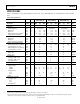
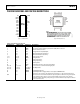
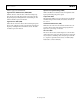
EQUIVALENT CIRCUITS
02874-A-005
AVDD
MODE
Figure 5. Equivalent Analog Input Circuit
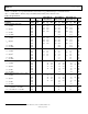
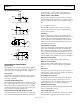
02874-A-006
AVDD
MODE
20kΩ
Figure 6. Equivalent MODE Input Circuit
02874-A-007
D9–D0,
OR
DRVDD
Figure 7. Equivalent Digital Output Circuit
02874-A-008
2.6kΩ
2.6kΩ
AVDD
CLK
Figure 8. Equivalent Digital Input Circuit
DEFINITIONS OF SPECIFICATIONS
Aperture Delay
Aperture delay is a measure of the sample-and-hold amplifier
(SHA) performance and is measured from the rising edge of the
clock input to when the input signal is held for conversion.
Aperture Jitter
Aperture jitter is the variation in aperture delay for successive
samples and can be manifested as frequency-dependent noise
on the input to the ADC.
Clock Pulse Width and Duty Cycle
Pulse width high is the minimum amount of time that the clock
pulse should be left in the Logic 1 state to achieve rated perfor-
mance. Pulse width low is the minimum time the clock pulse
should be left in the low state. At a given clock rate, these speci-
fications define an acceptable clock duty cycle.
Differential Nonlinearity (DNL, No Missing Codes)
An ideal ADC exhibits code transitions that are exactly 1 LSB
apart. DNL is the deviation from this ideal value. Guaranteed
no missing codes to 10-bit resolution indicate that all 1024
codes, respectively, must be present over all operating ranges.
Effective Number of Bits (ENOB)
For a sine wave, SINAD can be expressed in terms of the num-
ber of bits. Using the following formula, it is possible to obtain a
measure of performance expressed as N, the effective number of
bits
N = (SINAD – 1.76)/6.02
Thus, the effective number of bits for a device for sine wave
inputs at a given input frequency can be calculated directly
from its measured SINAD.
Gain Error
The first code transition should occur at an analog value 1/2
LSB above negative full scale. The last transition should occur at
an analog value 1 1/2 LSB below the positive full scale. Gain
error is the deviation of the actual difference between the first
and last code transitions and the ideal difference between the
first and last code transitions.
Integral Nonlinearity (INL)
INL refers to the deviation of each individual code from a line
drawn from “negative full scale” through “positive full scale.”
The point used as negative full scale occurs 1/2 LSB before the
first code transition. Positive full scale is defined as a level 1 1/2
LSB beyond the last code transition. The deviation is measured
from the middle of each particular code to the true straight line.
Maximum Conversion Rate
The clock rate at which parametric testing is performed.
Minimum Conversion Rate
The clock rate at which the SNR of the lowest analog signal
frequency drops by no more than 3 dB below the guaranteed
limit.
Offset Error
The major carry transition should occur for an analog value 1/2
LSB below VIN+ = VIN−. Zero error is defined as the deviation
of the actual transition from that point.
Out-of-Range Recovery Time
Out-of-range recovery time is the time it takes for the ADC to
reacquire the analog input after a transient from 10% above
positive full scale to 10% above negative full scale, or from 10%
below negative full scale to 10% below positive full scale.
Output Propagation Delay
The delay between the clock logic threshold and the time when
all bits are within valid logic levels.
Power Supply Rejection
The specification shows the maximum change in full scale from
the value with the supply at the minimum limit to the value