Quad, 10-Bit, 40/65 MSPS Serial LVDS 1.8 V ADC AD9219 Data Sheet 4 ADCs integrated into 1 package 94 mW ADC power per channel at 65 MSPS SNR = 60 dB (to Nyquist) ENOB = 9.7 bits SFDR = 78 dBc (to Nyquist) Excellent linearity DNL = ±0.2 LSB (typical) INL = ±0.3 LSB (typical) Serial LVDS (ANSI-644, default) Low power, reduced signal option (similar to IEEE 1596.3) Data and frame clock outputs 315 MHz full-power analog bandwidth 2 V p-p input voltage range 1.
AD9219 Data Sheet TABLE OF CONTENTS Features .............................................................................................. 1 Analog Input Considerations ................................................... 20 Applications ....................................................................................... 1 Clock Input Considerations ...................................................... 23 General Description .........................................................................
Data Sheet AD9219 Changes to RBIAS Pin Section ......................................................28 Changes to Figure 67 ......................................................................29 Changes to Hardware Interface Section .......................................30 Added Figure 68 ..............................................................................31 Changes to Table 15 ........................................................................
AD9219 Data Sheet SPECIFICATIONS AVDD = 1.8 V, DRVDD = 1.8 V, 2 V p-p differential input, 1.0 V internal reference, AIN = −0.5 dBFS, unless otherwise noted. Table 1. Parameter1 RESOLUTION ACCURACY No Missing Codes Offset Error Offset Matching Gain Error Gain Matching Differential Nonlinearity (DNL) Integral Nonlinearity (INL) TEMPERATURE DRIFT Offset Error Gain Error Reference Voltage (1 V Mode) REFERENCE Output Voltage Error (VREF = 1 V) Load Regulation at 1.
Data Sheet AD9219 AC SPECIFICATIONS AVDD = 1.8 V, DRVDD = 1.8 V, 2 V p-p differential input, 1.0 V internal reference, AIN = −0.5 dBFS, unless otherwise noted. Table 2. Parameter1 SIGNAL-TO-NOISE RATIO (SNR) fIN = 2.4 MHz fIN = 19.7 MHz fIN = 35 MHz fIN = 70 MHz SIGNAL-TO-NOISE AND DISTORTION RATIO (SINAD) fIN = 2.4 MHz fIN = 19.7 MHz fIN = 35 MHz fIN = 70 MHz EFFECTIVE NUMBER OF BITS (ENOB) fIN = 2.4 MHz fIN = 19.7 MHz fIN = 35 MHz fIN = 70 MHz SPURIOUS-FREE DYNAMIC RANGE (SFDR) fIN = 2.4 MHz fIN = 19.
AD9219 Data Sheet DIGITAL SPECIFICATIONS AVDD = 1.8 V, DRVDD = 1.8 V, 2 V p-p differential input, 1.0 V internal reference, AIN = −0.5 dBFS, unless otherwise noted. Table 3.
Data Sheet AD9219 SWITCHING SPECIFICATIONS AVDD = 1.8 V, DRVDD = 1.8 V, 2 V p-p differential input, 1.0 V internal reference, AIN = −0.5 dBFS, unless otherwise noted. Table 4.
AD9219 Data Sheet TIMING DIAGRAMS N–1 VIN ± x tA N tEL tEH CLK– CLK+ tCPD DCO– DCO+ tFRAME tFCO FCO– FCO+ tPD tDATA D–x MSB N–9 D8 N–9 D7 N–9 D6 N–9 D5 N–9 D4 N–9 D3 N–9 D2 N–9 D1 N–9 D0 N–9 MSB N–8 D8 N–8 D7 N–8 D6 N–8 D5 N–8 05726-040 D+x Figure 2. 10-Bit Data Serial Stream, MSB First (Default) N–1 VIN ± x tA N tEH CLK– tEL CLK+ tCPD DCO– DCO+ tFRAME tFCO FCO– FCO+ tPD tDATA MSB N–9 D10 N–9 D9 N–9 D8 N–9 D7 N–9 D6 N–9 D5 N–9 D+x Figure 3.
Data Sheet AD9219 N–1 VIN ± x tA N tEL tEH CLK– CLK+ tCPD DCO– DCO+ tFRAME tFCO FCO– FCO+ tPD tDATA D–x D0 N–9 D1 N–9 D2 N–9 D3 N–9 D4 N–9 D5 N–9 D6 N–9 D7 N–9 D8 N–9 LSB N–8 D0 N–8 D1 N–8 D2 N–8 05726-041 LSB N–9 D+x Figure 4. 10-Bit Stream, LSB First Rev.
AD9219 Data Sheet ABSOLUTE MAXIMUM RATINGS Table 5. Parameter ELECTRICAL AVDD DRVDD AGND AVDD Digital Outputs (D + x, D − x, DCO+, DCO−, FCO+, FCO−) CLK+, CLK− VIN + x, VIN − x SDIO/ODM PDWN, SCLK/DTP, CSB REFT, REFB, RBIAS VREF, SENSE ENVIRONMENTAL Operating Temperature Range (Ambient) Maximum Junction Temperature Lead Temperature (Soldering, 10 sec) Storage Temperature Range (Ambient) With Respect To Rating AGND DRGND DRGND DRVDD DRGND −0.3 V to +2.0 V −0.3 V to +2.0 V −0.3 V to +0.3 V −2.0 V to +2.
Data Sheet AD9219 VIN + C AVDD AVDD REFT REFB VREF SENSE RBIAS AVDD VIN + B VIN – B 46 45 44 43 42 41 40 39 38 37 PIN 1 INDICATOR AVDD 1 36 AVDD AVDD 2 35 AVDD VIN – D 3 34 VIN – A 33 VIN + A 5 32 AVDD AVDD 6 31 PDWN 30 CSB 8 29 SDIO/ODM AVDD 9 28 SCLK/DTP AVDD 10 27 AVDD 11 26 DRGND DRVDD 12 25 DRVDD EXPOSED PADDLE, PIN 0 (BOTTOM OF PACKAGE) VIN + D 4 AD9219 DCO+ 24 23 DCO– 21 FCO– FCO+ 22 D + A 20 17 D–B D + C 16 15 D–C D–D 13 DRGN
AD9219 Pin No.
Data Sheet AD9219 EQUIVALENT CIRCUITS DRVDD V V D– VIN ± x D+ DRGND Figure 6. Equivalent Analog Input Circuit CLK+ V 05726-005 05726-030 V Figure 9. Equivalent Digital Output Circuit 10Ω 10kΩ 1.25V 10kΩ SCLK/DTP AND PDWN 10Ω 1kΩ 30kΩ 05726-033 05726-032 CLK– Figure 7. Equivalent Clock Input Circuit Figure 10. Equivalent SCLK/DTP and PDWN Input Circuit RBIAS 350Ω 05726-031 30kΩ 05726-035 SDIO/ODM 100Ω Figure 8. Equivalent SDIO/ODM Input Circuit Figure 11.
AD9219 Data Sheet AVDD 70kΩ CSB 1kΩ 6kΩ Figure 12. Equivalent CSB Input Circuit Figure 14. Equivalent VREF Circuit 1kΩ 05726-036 SENSE 05726-037 05726-034 VREF Figure 13. Equivalent SENSE Circuit Rev.
Data Sheet AD9219 TYPICAL PERFORMANCE CHARACTERISTICS 0 0 AIN = –0.5dBFS SNR = 61.22dB ENOB = 9.88 BITS SFDR = 85.20dBc –40 –60 –80 –100 –40 –60 –80 0 2 4 6 8 10 12 14 16 18 –120 20 05726-058 –100 05726-056 –120 AIN = –0.5dBFS SNR = 59.81dB ENOB = 9.64 BITS SFDR = 70.02dBc –20 AMPLITUDE (dBFS) AMPLITUDE (dBFS) –20 0 5 10 FREQUENCY (MHz) Figure 15. Single-Tone 32k FFT with fIN = 2.
AD9219 Data Sheet 90 0 AIN = –0.5dBFS SNR = 56.72dB ENOB = 9.13 BITS SFDR = 66.41dBc –20 85 2V p-p, SFDR –40 SNR/SFDR (dB) AMPLITUDE (dBFS) 80 –60 –80 75 70 65 60 2V p-p, SNR –100 0 5 10 15 20 25 50 10 30 05726-063 05726-054 –120 55 15 Figure 21. Single-Tone 32k FFT with fIN = 190 MHz, fSAMPLE = 65 MSPS 25 30 35 40 Figure 24. SNR/SFDR vs. Encode, fIN = 35 MHz, fSAMPLE = 40 MSPS 90 0 AIN = –0.5dBFS SNR = 58.57dB ENOB = 9.44 BITS SFDR = 57.
Data Sheet AD9219 100 100 2V p-p, SFDR 60 50 2V p-p, SNR 40 70dB REFERENCE 30 2V p-p, SFDR 60 50 2V p-p, SNR 40 70dB REFERENCE 30 20 05726-062 20 10 0 –60 fIN = 35MHz fSAMPLE = 65MSPS 80 70 70 SNR/SFDR (dB) 90 fIN = 10.3MHz fSAMPLE = 40MSPS –50 –40 –30 –20 –10 05726-067 80 SNR/SFDR (dB) 90 10 0 –60 0 –50 Figure 27. SNR/SFDR vs. Analog Input Level, fIN = 10.
AD9219 Data Sheet 0 90 AIN1 AND AIN2 = –7dBFS SFDR = 78.53dBc IMD2 = 78.61dBc IMD3 = 78.17dBc –20 85 2V p-p, SFDR SINAD/SFDR (dB) AMPLITUDE (dBFS) 80 –40 –60 –80 75 70 65 2V p-p, SINAD 60 –100 0 5 10 15 20 25 50 –40 30 05726-069 05726-050 –120 55 –20 FREQUENCY (MHz) 40 60 80 Figure 36. SINAD/SFDR vs. Temperature, fIN = 10.3 MHz, fSAMPLE = 65 MSPS 1.0 0 AIN1 AND AIN2 = –7dBFS SFDR = 74.90dBc IMD2 = 83.52dBc IMD3 = 74.56dBc –20 0.8 0.6 0.4 –40 INL (LSB) –60 –80 0.2 0 –0.
Data Sheet AD9219 0 –45.5 –20 AMPLITUDE (dBFS) –45.0 –46.5 –47.0 –47.5 –40 –60 –80 –48.0 10 05726-082 –100 15 20 25 30 35 40 45 –120 50 05726-051 CMRR (dB) –46.0 NPR = 51.72dB NOTCH = 18.0MHz NOTCH WIDTH = 3.0MHz 0 5 10 1.2 25 30 0 0 LSB rms –1 FUNDAMENTAL LEVEL (dB) 1.0 0.8 0.6 0.4 –2 –3dB CUTOFF = 315MHz –3 –4 –5 –6 –7 N–3 N–2 N–1 N N+1 N+2 N+3 CODE 05726-084 –8 0.2 05726-080 NUMBER OF HITS (Millions) 20 Figure 41.
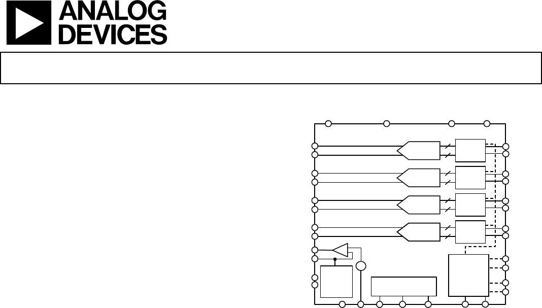
AD9219 Data Sheet THEORY OF OPERATION The AD9219 architecture consists of a pipelined ADC divided into three sections: a 4-bit first stage followed by eight 1.5-bit stages and a final 3-bit flash. Each stage provides sufficient overlap to correct for flash errors in the preceding stage. The quantized outputs from each stage are combined into a final 10-bit result in the digital correction logic.
Data Sheet AD9219 90 80 75 85 SFDR (dBc) SFDR (dBc) 80 60 SNR (dB) 55 75 70 65 SNR (dB) 50 60 45 55 40 0 0.2 0.4 0.6 0.8 1.0 1.2 1.4 50 0.2 1.6 ANALOG INPUT COMMON-MODE VOLTAGE (V) 0.4 0.6 0.8 1.0 1.2 1.4 1.6 ANALOG INPUT COMMON-MODE VOLTAGE (V) Figure 44. SNR/SFDR vs. Common-Mode Voltage, fIN = 2.4 MHz, fSAMPLE = 65 MSPS Figure 46. SNR/SFDR vs. Common-Mode Voltage, fIN = 2.
AD9219 Data Sheet ADT1-1WT 1:1 Z RATIO For best dynamic performance, the source impedances driving VIN + x and VIN − x should be matched such that commonmode settling errors are symmetrical. These errors are reduced by the common-mode rejection of the ADC. An internal reference buffer creates the positive and negative reference voltages, REFT and REFB, respectively, that define the span of the ADC core.
Data Sheet AD9219 Figure 52 shows a preferred method for clocking the AD9219. The low jitter clock source is converted from a single-ended signal to a differential signal using an RF transformer. The back-toback Schottky diodes across the secondary transformer limit clock excursions into the AD9219 to approximately 0.8 V p-p differential.
AD9219 Data Sheet Clock Jitter Considerations Power Dissipation and Power-Down Mode High speed, high resolution ADCs are sensitive to the quality of the clock input. The degradation in SNR at a given input frequency (fA) due only to aperture jitter (tJ) can be calculated by As shown in Figure 58 and Figure 59, the power dissipated by the AD9219 is proportional to its sample rate.
Data Sheet AD9219 By asserting the PDWN pin high, the AD9219 is placed into power-down mode. In this state, the ADC typically dissipates 3 mW. During power-down, the LVDS output drivers are placed into a high impedance state. If any of the SPI features are changed before the power-down feature is enabled, the chip continues to function after PDWN is pulled low without requiring a reset. The AD9219 returns to normal operating mode when the PDWN pin is pulled low. This pin is both 1.8 V and 3.3 V tolerant.
AD9219 Data Sheet EYE: ALL BITS ULS: 10000/15600 EYE: ALL BITS 400 EYE DIAGRAM VOLTAGE (V) EYE DIAGRAM VOLTAGE (V) 500 0 ULS: 9599/15599 200 0 –200 –400 –500 –1ns –0.5ns 0ns 0.5ns –1ns 1ns –0.5ns 0ns 0.5ns 1ns 50 0 –100ps 0ps 100ps 0 –150ps Figure 61.
Data Sheet AD9219 Two output clocks are provided to assist in capturing data from the AD9219. The DCO is used to clock the output data and is equal to five times the sample clock (CLK) rate. Data is clocked out of the AD9219 and must be captured on the rising and falling edges of the DCO that supports double data rate (DDR) capturing. The FCO is used to signal the start of a new output byte and is equal to the sample clock rate. See the timing diagram shown in Figure 2 for more information. Table 9.
AD9219 Data Sheet When the SPI is used, the DCO phase can be adjusted in 60° increments relative to the data edge. This enables the user to refine system timing margins if required. The default DCO+ and DCO− timing, as shown in Figure 2, is 90° relative to the output data edge. An 8-, 12-, or 14-bit serial stream can also be initiated from the SPI. This allows the user to implement and test compatibility with lower and higher resolution systems.
Data Sheet AD9219 SCLK/DTP Pin RBIAS Pin The SCLK/DTP pin is for use in applications that do not require SPI mode operation. This pin can enable a single digital test pattern if it and the CSB pin are held high during device powerup. When SCLK/DTP is tied to AVDD, the ADC channel outputs shift out the following pattern: 1000 0000 0000. The FCO and DCO function normally while all channels shift out the repeatable test pattern.
AD9219 Data Sheet Internal Reference Operation External Reference Operation A comparator within the AD9219 detects the potential at the SENSE pin and configures the reference. If SENSE is grounded, the reference amplifier switch is connected to the internal resistor divider (see Figure 64), setting VREF to 1 V. The use of an external reference may be necessary to enhance the gain accuracy of the ADC or to improve thermal drift characteristics.
Data Sheet AD9219 SERIAL PORT INTERFACE (SPI) The AD9219 serial port interface allows the user to configure the converter for specific functions or operations through a structured register space provided in the ADC. This may provide the user with additional flexibility and customization, depending on the application. Addresses are accessed via the serial port and can be written to or read from via the port.
1.800 1.795 1.790 1.785 1.780 1.775 1.770 1.765 1.760 1.755 1.750 1.745 1.740 1.735 1.730 1.725 1.720 1.715 Data Sheet If the user chooses not to use the SPI, these dual-function pins serve their secondary functions when the CSB is strapped to AVDD during device power-up. See the Theory of Operation section for details on which pin-strappable functions are supported on the SPI pins.
Data Sheet AD9219 MEMORY MAP READING THE MEMORY MAP TABLE RESERVED LOCATIONS Each row in the memory map register table (Table 16) has eight address locations. The memory map is divided into three sections: the chip configuration register map (Address 0x00 to Address 0x02), the device index and transfer register map (Address 0x05 and Address 0xFF), and the ADC functions register map (Address 0x08 to Address 0x22).
AD9219 Data Sheet Table 16. Memory Map Register Addr.
Data Sheet AD9219 Addr. (Hex) 14 Register Name output_mode (MSB) Bit 7 X 15 output_adjust 16 Bit 5 X X Bit 6 0 = LVDS ANSI-644 (default) 1 = LVDS low power (IEEE1596.
AD9219 Data Sheet Power and Ground Recommendations Exposed Paddle Thermal Heat Slug Recommendations When connecting power to the AD9219, it is recommended that two separate 1.8 V supplies be used: one for analog (AVDD) and one for digital (DRVDD). If only one supply is available, it should be routed to the AVDD first and then tapped off and isolated with a ferrite bead or a filter choke preceded by decoupling capacitors for the DRVDD.
Data Sheet AD9219 EVALUATION BOARD each section. At least one 1.8 V supply is needed for AVDD_DUT and DRVDD_DUT; however, it is recommended that separate supplies be used for analog and digital signals and that each supply have a current capability of 1 A. To operate the evaluation board using the VGA option, a separate 5.0 V analog supply (AVDD_5 V) is needed. To operate the evaluation board using the SPI and alternate clock options, a separate 3.3 V analog supply (AVDD_3.
AD9219 Data Sheet DEFAULT OPERATION AND JUMPER SELECTION SETTINGS A differential LVPECL clock can also be used to clock the ADC input using the AD9515 (U202). Populate R225 and R227 with 0 Ω resistors and remove R217 and R218 to disconnect the default clock path inputs. In addition, populate C207 and C208 with a 0.1 μF capacitor and remove C210 and C211 to disconnect the default clock path outputs. The AD9515 has many pin-strappable options that are set to a default mode of operation.
Data Sheet AD9219 ALTERNATIVE ANALOG INPUT DRIVE CONFIGURATION The following is a brief description of the alternative analog input drive configuration using the AD8332 dual VGA. If this drive option is in use, some components may need to be populated, in which case all the necessary components are listed in Table 17. For more details on the AD8332 dual VGA, including how it works and its optional pin settings, consult the AD8332 data sheet.
AD9219 Data Sheet AVDD_DUT R105 DNP CH_A P102 VGA INPUT CONNECTION DNP INH1 AIN CHANNEL A R101 P101 DNP AIN R103 R102 0Ω 64.9Ω C101 0.1µF R104 0Ω R152 DNP FB102 R108 10Ω 33Ω T101 6 1 R106 DNP 5 CM1 2 CM1 4 3 VIN_A R161 499Ω C103 DNP C104 2.2pF R109 1kΩ FB103 R110 33Ω 10Ω C105 DNP R156 DNP R107 DNP R113 FB101 DNP 10Ω C102 0.1µF CH_A CM1 VIN_A E101 AVDD_DUT R111 1kΩ R112 1kΩ C106 DNP C107 0.1µF AVDD_DUT AVDD_DUT CH_B R153 DNP FB105 R121 10Ω 33Ω T102 6 1 FB104 10Ω C108 0.
P201 ENCODE INPUT ENC DNP P203 CLOCK CIRCUIT ENC AVDD AVDD VIN – D VIN + D AVDD AVDD CLK– CLK+ AVDD AVDD DRGND DRVDD C224 0.1µF R216 0Ω 2 R201 10kΩ AVDD AVDD VIN – A VIN + A AVDD PDWN C216 0.1µF R218 0Ω R217 0Ω OPT_CLK OPT_CLK 5 6 2 1 R221 10kΩ 1 1 U202 J201 J202 1 CR201 HSMS2812 S10 S9 S8 S7 S6 S5 S4 S3 S2 S1 S0 DNP: DO NOT POPULATE DNP DNP R235 DNP R236 DNP R237 0Ω DNP R234 DNP VREF SELECT 3 3 C211 0.1µF C210 0.1µF 19 18 22 23 R240 243Ω C209 0.1µF DNP C208 0.
CH_C CH_D POPULATE L301-L308 WITH 0Ω RESISTORS OR DESIGN YOUR OWN FILTER. CH_C Data Sheet CH_D AD9219 R301 DNP R302 DNP L306 L307 0Ω 0Ω 16 15 14 13 12 11 10 9 C321 0.1µF AVDD_5V R314 10kΩ DNP VG C313 0.1µF C314 0.1µF 6 7 8 INH2 VPS2 LON2 RCLMP GAIN MODE VCM2 VIN2 VIP2 COM2 LOP2 RCLAMP PIN HILO PIN = LO = ±50mV HILO PIN = H = ±75mV R311 10kΩ DNP C310 0.1µF 19 18 17 VOL2 VOH2 COMM 20 LMD1 LMD2 4 5 R310 187Ω R317 274Ω C322 0.018µF C325 0.
OPTIONAL VGA DRIVE CIRCUIT FOR CHANNEL A AND CHANNEL B R414 10kΩ C413 10µF C410 0.1µF C409 0.1µF C414 0.1µF R411 10kΩ 25 26 27 28 29 30 31 32 CH_B ENBV ENBL HILO VCM1 VIN1 VIP1 COM1 LOP1 U401 R407 187Ω C405 0.1µF R408 187Ω R405 374Ω C415 0.018µF R415 274Ω Figure 76. Evaluation Board Schematic, Optional DUT Analog Input Drive and SPI Interface Circuit (Continued) L409 120nH C416 0.1µF INH2 C419 0.1µF AD8332 R409 187Ω C422 0.1µF L410 120nH C421 22pF INH1 C417 0.
1 3 2 + C501 10µF 3.3V_AVDD DUT_DRVDD P4 4 P5 5 P6 6 P7 7 3 INPUT L501 10µH L508 10µH L502 10µH L503 10µH OUTPUT4 OUTPUT4 OUTPUT1 2 4 4 2 2 L505 10µH C513 1µF L504 10µH AVDD_5V +3.3V AVDD_3.3V +1.8V AVDD_DUT +5.0V R501 261Ω DUT_DRVDD DUT_AVDD C507 0.1µF C534 1µF PWR_IN C532 1µF PWR_IN 3 3 C517 0.1µF C525 0.1µF C527 0.1µF C519 0.1µF INPUT 2 OUTPUT4 4 OUTPUT1 2 OUTPUT4 4 OUTPUT1 ADP3339AKC-5 U504 INPUT ADP3339AKC-3.3 U502 C516 0.1µF C524 0.1µF C526 0.
AD9219 05726-020 Data Sheet Figure 78. Evaluation Board Layout, Primary Side Rev.
Data Sheet 05726-021 AD9219 Figure 79. Evaluation Board Layout, Ground Plane Rev.
AD9219 05726-022 Data Sheet Figure 80. Evaluation Board Layout, Power Plane Rev.
Data Sheet 05726-023 AD9219 Figure 81. Evaluation Board Layout, Secondary Side (Mirrored Image) Rev.
Data Sheet AD9219 Table 17. Evaluation Board Bill of Materials (BOM)1 Device PCB Capacitor Package PCB 402 Value PCB 0.
AD9219 Data Sheet Device Ferrite bead Package 603 Value 10 Ω, test freq 100 MHz, 25% tol, 500 mA Manufacturer Murata Manufacturer’s Part Number BLM18BA100SN1B 1 Reference Designator FB101, FB102, FB103, FB104, FB105, FB106, FB107, FB108, FB109, FB110, FB111, FB112 JP301 Connector 2-pin Samtec TSW-102-07-G-S 21 2 J205, J402 Connector 3-pin Samtec TSW-103-07-G-S 22 1 J201 to J204 Connector 12-pin Samtec TSW-104-08-G-T 23 1 J401 Connector 10-pin Samtec TSW-105-08-G-D 24 8 L50
Data Sheet AD9219 Item 37 Qty.
AD9219 Data Sheet Item 59 60 Qty. 1 1 Reference Designator U502 U201 Device IC IC Package SOT-223 LFCSP, CP-48-1 61 1 U203 IC SOT-23 62 1 U202 IC 63 1 U403 IC 64 1 U404 IC 65 1 U402 IC LFCSP CP-32-2 SC70, MAA06A SC70, MAA06A 8-SOIC 1 Value ADP3339AKC-3.3 AD9219BCPZ-65, quad, 10-bit, 65 MSPS serial LVDS 1.8 V ADC ADR510ARTZ, 1.0 V, precision low noise shunt voltage reference AD9515BCPZ Manufacturer Analog Devices Analog Devices Manufacturer’s Part Number ADP3339AKCZ-3.
Data Sheet AD9219 OUTLINE DIMENSIONS 0.30 0.23 0.18 0.60 MAX 0.60 MAX 37 36 PIN 1 INDICATOR 6.85 6.75 SQ 6.65 48 0.50 REF 1.00 0.85 0.80 12° MAX 0.80 MAX 0.65 TYP 13 12 0.22 MIN 5.50 REF 0.05 MAX 0.02 NOM COPLANARITY 0.08 0.20 REF SEATING PLANE 5.50 SQ 5.45 (BOTTOM VIEW) 0.50 0.40 0.30 PIN 1 INDICATOR *5.55 EXPOSED PAD 25 24 TOP VIEW 1 FOR PROPER CONNECTION OF THE EXPOSED PAD, REFER TO THE PIN CONFIGURATION AND FUNCTION DESCRIPTIONS SECTION OF THIS DATA SHEET.
AD9219 Data Sheet NOTES Rev.
Data Sheet AD9219 NOTES Rev.
AD9219 Data Sheet NOTES ©2006–2011 Analog Devices, Inc. All rights reserved. Trademarks and registered trademarks are the property of their respective owners. D05726-0-12/11(E) Rev.