
Datasheet


Table Of Contents
- Features
- Applications
- General Description
- Functional Block Diagram
- Product Highlights
- Revision History
- Specifications
- Timing Diagrams
- Absolute Maximum Ratings
- Pin Configuration and Function Descriptions
- Equivalent Circuits
- Typical Performance Characteristics
- Theory of Operation
- Serial Port Interface (SPI)
- Memory Map
- Evaluation Board
- Outline Dimensions
AD9219 Data Sheet
Rev. E | Page 22 of 56
For best dynamic performance, the source impedances driving
VIN + x and VIN − x should be matched such that common-
mode settling errors are symmetrical. These errors are reduced
by the common-mode rejection of the ADC. An internal
reference buffer creates the positive and negative reference
voltages, REFT and REFB, respectively, that define the span of
the ADC core. The output common-mode of the reference buffer
is set to midsupply, and the REFT and REFB voltages and span
are defined as
REFT = 1/2 (AVDD + VREF)
REFB = 1/2 (AVDD − VREF)
Span = 2 × (REFT − REFB) = 2 × VREF
It can be seen from these equations that the REFT and REFB
voltages are symmetrical about the midsupply voltage and, by
definition, the input span is twice the value of the VREF voltage.
Maximum SNR performance is achieved by setting the ADC to
the largest span in a differential configuration. In the case of the
AD9219, the largest input span available is 2 V p-p.
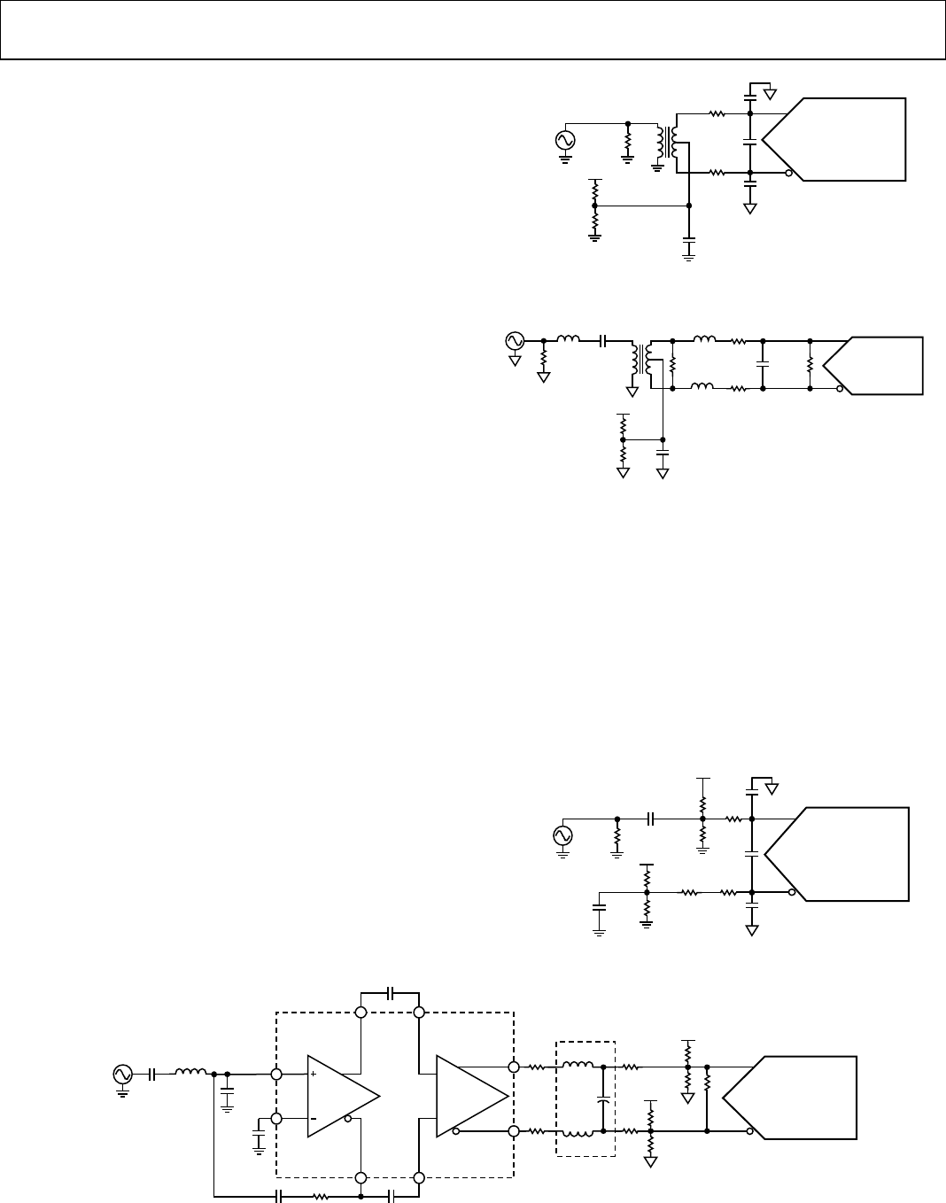
Differential Input Configurations
There are several ways to drive the AD9219 either actively or
passively; however, optimum performance is achieved by driving
the analog input differentially. For example, using the AD8332
differential driver to drive the AD9219 provides excellent perfor-
mance and a flexible interface to the ADC (see Figure 51) for
baseband applications. This configuration is commonly used
for medical ultrasound systems.
For applications where SNR is a key parameter, differential
transformer coupling is the recommended input configuration
(see Figure 48 and Figure 49), because the noise performance of
most amplifiers is not adequate to achieve the true performance
of the AD9219.
Regardless of the configuration, the value of the shunt capacitor,
C, is dependent on the input frequency and may need to be
reduced or removed.
2V p-p
R
R
*C
DIFF
C
*C
DIFF IS OPTIONAL
49.9
0.1F
1k
1k
AGND
AVDD
A
DT1-1WT
1:1 Z RATIO
VIN – x
ADC
AD9219
VIN + x
C
05726-008
Figure 48. Differential Transformer-Coupled Configuration
for Baseband Applications
ADC
AD9219
2V p-p
2.2pF 1k
0.1F
1k
1k
AVDD
A
DT1-1WT
1:1 Z RATIO
16nH
16nH
0.1F
16nH
33
33
499
65
VIN + x
VIN – x
05726-047
Figure 49. Differential Transformer-Coupled Configuration
for IF Applications
Single-Ended Input Configuration
A single-ended input may provide adequate performance in cost-
sensitive applications. In this configuration, SFDR and distortion
performance degrade due to the large input common-mode swing.
If the application requires a single-ended input configuration,
ensure that the source impedances on each input are well matched
in order to achieve the best possible performance. A full-scale
input of 2 V p-p can be applied to the ADC’s VIN + x pin while the
VIN − x pin is terminated. Figure 50 details a typical single-
ended input configuration.
2
V p-
p
R
R
49.9
0.1µF
0.1µF
AVDD
1k
25
1k
1k
A
V
DD
VIN – x
ADC
AD9219
VIN + x
*C
DIFF
C
*C
DIFF IS OPTIONAL
C
0
5726-009
Figure 50. Single-Ended Input Configuration
AD8332
1k
187
187
0.1
F
0.1F
0.1F
1V p-p
0.1F
LNA
120nH
VGA
VOH
VIP
INH
22pF
LMD
VIN
LOP
LON
VOL
18nF
274
VIN – x
ADC
AD9219
VIN + x
05726-007
LPF
+
68pF
33
33
AVDD
AVDD
680nH
680nH
10k
10k
10k
10k
Figure 51. Differential Input Configuration Using the AD8332 with Two-Pole, 16 MHz Low-Pass Filter