
Datasheet


Table Of Contents
- Features
- Applications
- General Description
- Functional Block Diagram
- Product Highlights
- Revision History
- Specifications
- Timing Diagrams
- Absolute Maximum Ratings
- Pin Configuration and Function Descriptions
- Equivalent Circuits
- Typical Performance Characteristics
- Theory of Operation
- Serial Port Interface (SPI)
- Memory Map
- Evaluation Board
- Outline Dimensions
AD9219 Data Sheet
Rev. E | Page 24 of 56
Clock Jitter Considerations
High speed, high resolution ADCs are sensitive to the quality of the
clock input. The degradation in SNR at a given input frequency (f
A
)
due only to aperture jitter (t
J
) can be calculated by
SNR Degradation = 20 × log 10(1/2 × π × f
A
× t
J
)
In this equation, the rms aperture jitter represents the root mean
square of all jitter sources, including the clock input, analog input
signal, and ADC aperture jitter. IF undersampling applications
are particularly sensitive to jitter (see Figure 57).
The clock input should be treated as an analog signal in cases
where aperture jitter may affect the dynamic range of the AD9219.
Power supplies for clock drivers should be separated from the
ADC output driver supplies to avoid modulating the clock signal
with digital noise. Low jitter, crystal-controlled oscillators are
the best clock sources. If the clock is generated from another type
of source (by gating, dividing, or another method), it should be
retimed by the original clock during the last step.
Refer to the AN-501 Application Note and to the AN-756
Application Note for more in-depth information about jitter
performance as it relates to ADCs at www.analog.com.
1 10 100 1000
16 BITS
14 BITS
12 BITS
30
40
50
60
70
80
90
100
110
120
130
0.125 ps
0.25 ps
0.5 ps
1.0 ps
2.0 ps
ANALOG INPUT FREQUENCY (MHz)
10 BITS
05726-038
RMS CLOCK JITTER REQUIREMENT
SNR (dB)
Figure 57. Ideal SNR vs. Input Frequency and Jitter
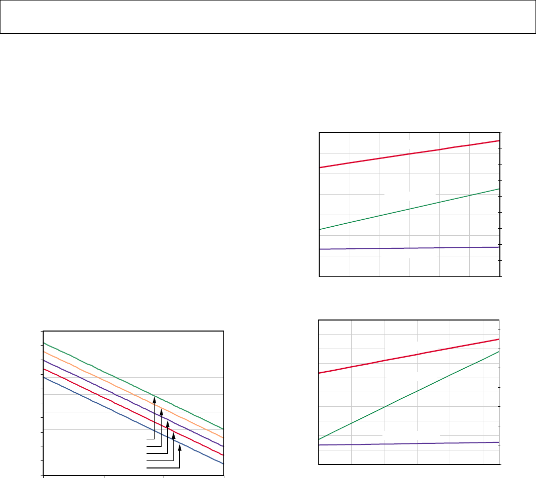
Power Dissipation and Power-Down Mode
As shown in Figure 58 and Figure 59, the power dissipated by
the AD9219 is proportional to its sample rate. The digital power
dissipation does not vary significantly because it is determined
primarily by the DRVDD supply and bias current of the LVDS
output drivers.
05726-074
CURRENT (mA)
POWER (mW)
ENCODE (MSPS)
AVDD CURRENT
TOTAL POWER
DRVDD CURRENT
180
200
220
240
260
280
300
320
340
360
0
20
40
60
80
100
120
140
15 20 25 30 35 40
10
Figure 58. Supply Current vs. f
SAMPLE
for f
IN
= 10.3 MHz, f
SAMPLE
= 40 MSPS
0
05726-078
CURRENT (mA)
POWER (mW)
ENCODE (MSPS)
AVDD CURRENT
TOTAL POWER
DRVDD CURRENT
20
40
60
80
100
120
140
160
180
200
10 20 30 40 50 60
250
270
290
310
330
350
370
390
Figure 59. Supply Current vs. f
SAMPLE
for f
IN
= 10.3 MHz, f
SAMPLE
= 65 MSPS