
Evaluation Board User Guide


UG-001 Evaluation Board User Guide
Rev. 0 | Page 10 of 24
Adjusting the Amplitude of the Input Signal
Next, adjust the amplitude of the input signal for each channel
as follows:
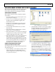
1. Adjust the amplitude of the input signal so that the
fundamental is at the desired level. (Examine the Fund
Power reading in the left panel of the VisualAnalog FFT
window.) If the gain pin voltage is too low, it is not possible
to reach full scale without distortion. Use a higher gain
setting or a lower input level to avoid distortion. This also
depends on the PGA gain setting, which can be 30 dB,
27 dB, 24 dB, or 21dB. See Figure 15 and Figure 16.
07782-026
Figure 15. VisualAnalog, Graph Window
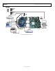
0
7782-027
Figure 16. VisualAnalog, Formatted FFT Plot
2. Repeat this procedure for the other seven channels.
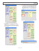
3. Click the disk icon within the Graph window to save the
performance plot. See Figure 17 for an example.
0
–130
02
07782-119
FREQUENCY (MHz)
AMPLITUDE (dBFS)
5
–10
–20
–30
–40
–50
–60
–70
–80
–90
–100
–110
–120
5101520
f
IN
= 3.5MHz @ –1dBFS
LNA = 6×
V
GAIN
= 1V
FILTER TUNED
HPF = 700kHz
Figure 17. Typical FFT, AD9272/AD9273
USING THE INTEGRATED CROSSPOINT SWITCH
(CW DOPPLER MODE)
To examine the spectrum of the CW Doppler integrated
crosspoint switch output, use the following procedure:
1. Complete the steps in the Configuring the Board and
Using the Software for Testing sections to ensure that the
board is set up correctly.
2. Optionally, remove the voltage source from the gain pin. It
does not affect the CW Doppler output.
3. Connect the dc voltage source to P601, connecting the
−5 V pin, the 0 V ground pin, and the +5 V pin as shown
in Figure 1. These benchtop linear supplies should each have
100 mA of current capability.
4. Place jumpers on the top pin pairs of P606 or P607 to
connect CWD2+/CWD2− to CWD5+/CWD5− to the
IOP/ION buses. This directs each of these connections to
the output amplifier for display.
Note that the CWD0±/CWD1±/CWD6±/CWD7± outputs
are configured and biased to interface with the AD8339
evaluation board. The AD9272/AD9273 is specially designed
to snap onto the AD8339 evaluation board to allow the user to
evaluate a larger portion of this common signal chain. For
detailed instructions about enabling this function, send an
email to highspeed.converters@analog.com.
5. Use a 1 m, shielded, RG-58, 50 Ω coaxial cable to connect
the spectrum analyzer to J402 (labeled AOUT on the
evaluation board).
6. In the ADCBase 0 tab of the SPI Controller, find the
MODES(8) box. Select the CW Mode option (see Figure 18).