
Datasheet


AD9522-1
Rev. 0 | Page 11 of 84
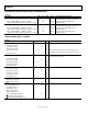
CLOCK OUTPUT ABSOLUTE TIME JITTER (CLOCK GENERATION USING EXTERNAL VCXO)
Table 10.
Parameter Min Typ Max Unit Test Conditions/Comments
LVDS OUTPUT ABSOLUTE TIME JITTER
Application example based on a typical setup using an
external 245.76 MHz VCXO (Toyocom TCO-2112);
reference = 15.36 MHz; R DIV = 1
LVDS = 245.76 MHz; PLL LBW = 125 Hz 87 fs rms Integration BW = 200 kHz to 5 MHz
108 fs rms Integration BW = 200 kHz to 10 MHz
146 fs rms Integration BW = 12 kHz to 20 MHz
LVDS = 122.88 MHz; PLL LBW = 125 Hz 120 fs rms Integration BW = 200 kHz to 5 MHz
151 fs rms Integration BW = 200 kHz to 10 MHz
207 fs rms Integration BW = 12 kHz to 20 MHz
LVDS = 61.44 MHz; PLL LBW = 125 Hz 157 fs rms Integration BW = 200 kHz to 5 MHz
210 fs rms Integration BW = 200 kHz to 10 MHz
295 fs rms Integration BW = 12 kHz to 20 MHz
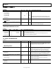
CLOCK OUTPUT ADDITIVE TIME JITTER (VCO DIVIDER NOT USED)
Table 11.
Parameter Min Typ Max Unit Test Conditions/Comments
LVDS OUTPUT ADDITIVE TIME JITTER
Distribution section only; does not include
PLL and VCO; measured at rising edge of
clock signal
CLK = 622.08 MHz 69 fs rms Integration bandwidth = 12 kHz to 20 MHz
Any LVDS Output = 622.08 MHz
Divide Ratio = 1
CLK = 622.08 MHz 116 fs rms Integration bandwidth = 12 kHz to 20 MHz
Any LVDS Output = 155.52 MHz
Divide Ratio = 4
CLK = 100 MHz 263 fs rms Calculated from SNR of ADC method
Any LVDS Output = 100 MHz Broadband jitter
Divide Ratio = 1
CLK = 500 MHz 242 fs rms Calculated from SNR of ADC method
Any LVDS Output = 100 MHz Broadband jitter
Divide Ratio = 5
CMOS OUTPUT ADDITIVE TIME JITTER
Distribution section only; does not include
PLL and VCO
CLK = 200 MHz 289 fs rms Calculated from SNR of ADC method
Any CMOS Output Pair = 100 MHz Broadband jitter
Divide Ratio = 2