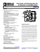
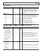
FEATURES FUNCTIONAL BLOCK DIAGRAM Output frequency: <1 MHz to 1 GHz Start-up frequency accuracy: <±100 ppm (determined by VCXO reference accuracy) Zero delay operation Input-to-output edge timing: <150 ps 14 outputs: configurable LVPECL, LVDS, HSTL, and LVCMOS 14 dedicated output dividers with jitter-free adjustable delay Adjustable delay: 63 resolution steps of ½ period of VCO output divider Output-to-output skew: <50 ps Duty-cycle correction for odd divider settings Automatic synchronization of all outp
AD9523 Data Sheet TABLE OF CONTENTS Features .............................................................................................. 1 Terminology .................................................................................... 19 Applications ....................................................................................... 1 Theory of Operation ...................................................................... 20 Functional Block Diagram ..........................................
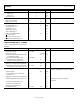
Data Sheet AD9523 REVISION HISTORY 2/13—Rev. B to Rev. C Deleted VDD1.8_PLL2................................................. Throughout Changes to Data Sheet Title ............................................................. 1 Added TJ of 115°C, Table 1 .............................................................. 4 Changed VDD3_PLL1, Supply Voltage for PLL1 Typical Parameter from 22 mA to 37 mA and Changed VDD3_PLL1, Supply Voltage for PLL1 Maximum Parameter from 25.2 mA to 43 mA, Table 2 ............
AD9523 Data Sheet SPECIFICATIONS fVCXO = 122.88 MHz single ended, REFA and REFB on differential at 30.72 MHz, fVCO = 3932.16 MHz, doubler is off, channel control low power mode off, divider phase =1, unless otherwise noted. Typical is given for VDD = 3.3 V ± 5%, and TA = 25°C, unless otherwise noted. Minimum and maximum values are given over the full VDD, and TA (−40°C to +85°C) variation, as listed in Table 1. CONDITIONS Table 1.
Data Sheet AD9523 POWER DISSIPATION Table 3. Parameter POWER DISSIPATION Typical Configuration Min PD, Power-Down INCREMENTAL POWER DISSIPATION Low Power Typical Configuration Output Distribution, Driver On LVDS LVPECL HSTL CMOS Typ Max Unit 876 970 mW 101 132.2 mW 389 450 mW 15.3 47.8 50.1 40.2 43.7 6.6 9.9 9.9 18.4 55.4 54.9 46.3 50.3 7.9 11.9 11.
AD9523 Data Sheet OSC_CTRL OUTPUT CHARACTERISTICS Table 5. Parameter OUTPUT VOLTAGE High Low Min Typ Max Unit Test Conditions/Comments V mV RLOAD > 20 kΩ 150 Max Unit Test Conditions/Comments 250 MHz V 0.8 V VDD3_PLL1 − 0.15 REF_TEST INPUT CHARACTERISTICS Table 6. Parameter REF_TEST INPUT Input Frequency Range Input High Voltage Min Typ 2.0 Input Low Voltage PLL1 CHARACTERISTICS Table 7.
Data Sheet AD9523 DISTRIBUTION OUTPUT CHARACTERISTICS (OUT0, OUT0 TO OUT13, OUT13) Duty cycle performance is specified with the invert divider bit set to 1, and the divider phase bits set to 0.5. (For example, for Channel 0, 0x190[7] = 1 and 0x192[7:2] = 1.) Output Voltage Reference VDD in Table 9 refers to the 3.3 VDD3_OUT[x:y] supply. Table 9.
AD9523 Data Sheet TIMING ALIGNMENT CHARACTERISTICS Table 10.
Data Sheet AD9523 LOGIC INPUT PINS—PD, EEPROM_SEL, REF_SEL, RESET, SYNC Table 13. Parameter VOLTAGE Input High Input Low INPUT LOW CURRENT CAPACITANCE RESET TIMING Pulse Width Low Inactive to Start of Register Programming SYNC TIMING Pulse Width Low Min Typ Max Unit ±80 0.8 ±250 V V µA 2.0 3 Test Conditions/Comments The minus sign indicates that, due to the internal pull-up resistor, current is flowing out of the AD9523 pF 50 100 ns ns 1.
AD9523 Parameter Current Input Logic 1 Input Logic 0 Input Capacitance SDIO, SDO (OUTPUTS) Output Logic 1 Voltage Output Logic 0 Voltage TIMING Clock Rate (SCLK, 1/tSCLK) Pulse Width High, tHIGH Pulse Width Low, tLOW SDIO to SCLK Setup, tDS SCLK to SDIO Hold, tDH SCLK to Valid SDIO and SDO, tDV CS to SCLK Setup, tS CS to SCLK Setup and Hold, tS, tC CS Minimum Pulse Width High, tPWH Data Sheet Min Typ Max 1 1 2 Unit Test Conditions/Comments µA µA pF 2.7 0.4 25 8 12 3.
Data Sheet Parameter SCL, SDA Fall Time, tFALL Data Setup Time, tSET; DAT Data Hold Time, tHLD; DAT Capacitive Load for Each Bus Line, CB1 1 2 AD9523 Min 20 + 0.1 CB1 100 100 Typ Max 300 880 Unit ns ns ns 400 pF Test Conditions/Comments This is a minor deviation from the original I²C specification of 0 ns minimum 2 CB is the capacitance of one bus line in picofarads (pF).
AD9523 Data Sheet ABSOLUTE MAXIMUM RATINGS Table 17. Parameter VDD3_PLL1, VDD3_PLL2, VDD3_REF, VDD3_OUT, LDO_VCO to GND REFA, REFA, REFIN, REFB, REFB to GND SCLK/SCL, SDIO/SDA, SDO, CS to GND OUT0, OUT0, OUT1, OUT1, OUT2, OUT2, OUT3, OUT3, OUT4, OUT4, OUT5, OUT5, OUT6, OUT6, OUT7, OUT7, OUT8, OUT8, OUT9, OUT9, OUT10, OUT10, OUT11, OUT11, OUT12, OUT12, OUT13, OUT13 to GND SYNC, RESET, PD to GND STATUS0, STATUS1 to GND SP0, SP1, EEPROM_SEL to GND VDD1.
Data Sheet AD9523 72 71 70 69 68 67 66 65 64 63 62 61 60 59 58 57 56 55 PLL1_OUT ZD_IN ZD_IN NC OUT0 OUT0 VDD3_OUT[0:1] OUT1 OUT1 VDD1.8_OUT[0:3] OUT2 OUT2 VDD3_OUT[2:3] OUT3 OUT3 EEPROM_SEL STATUS0/SP0 STATUS1/SP1 PIN CONFIGURATION AND FUNCTION DESCRIPTIONS 1 2 3 4 5 6 7 8 9 10 11 12 13 14 15 16 17 18 PIN 1 INDICATOR AD9523 (TOP VIEW) 54 53 52 51 50 49 48 47 46 45 44 43 42 41 40 39 38 37 VDD1.8_OUT[4:5] OUT4 OUT4 VDD3_OUT[4:5] OUT5 OUT5 VDD1.8_OUT[6:7] OUT6 OUT6 VDD3_OUT[6:7] OUT7 OUT7 VDD1.
AD9523 Data Sheet Pin No. 12 Mnemonic LDO_PLL2 Type1 P/O 13 14 VDD3_PLL2 LDO_VCO P P/O 15 16 17 PD REF_SEL SYNC I I I 18 19 VDD3_REF RESET P I 20 21 CS SCLK/SCL I I 22 23 SDIO/SDA SDO I/O O 24 25 REF_TEST OUT13 I O 26 OUT13 O 27 28 VDD3_OUT[12:13] OUT12 P O 29 OUT12 O 30 31 VDD1.8_OUT[12:13] OUT11 P O 32 OUT11 O 33 34 VDD3_OUT[10:11] OUT10 P O 35 OUT10 O 36 37 VDD1.8_OUT[10:11] OUT9 P O 38 OUT9 O 39 40 VDD3_OUT[8:9] OUT8 P O 41 OUT8 O 42 43 VDD1.
Data Sheet AD9523 Pin No. 46 Mnemonic OUT6 Type1 O 47 OUT6 O 48 49 VDD1.8_OUT[6:7] OUT5 P O 50 OUT5 O 51 52 VDD3_OUT[4:5] OUT4 P O 53 OUT4 O 54 55 VDD1.8_OUT[4:5] STATUS1/SP1 P I/O 56 STATUS0/SP0 I/O 57 EEPROM_SEL I 58 OUT3 O 59 OUT3 O 60 61 VDD3_OUT[2:3] OUT2 P O 62 OUT2 O 63 64 VDD1.
AD9523 Data Sheet TYPICAL PERFORMANCE CHARACTERISTICS fVCXO = 122.88 MHz, REFA differential at 30.72 MHz, fVCO = 3686.4 MHz, and doubler is off, unless otherwise noted. 60 35 50 30 25 40 CURRENT (mA) CURRENT (mA) HSTL = 16mA 20pF 30 HSTL = 8mA 20 10pF 2pF 20 15 10 10 0 0 200 400 600 800 1000 08439-006 08439-003 5 0 0 1200 100 FREQUENCY (MHz) 400 500 600 Figure 6. VDD3_OUT[x:y] Current (Typical) vs. Frequency; CMOS Mode, 20 pF, 10 pF, and 2 pF Load 45 3.
Data Sheet AD9523 1.4 –70 LVDS = 7mA PHASE NOISE (dBc/Hz) 0.8 LVDS = 3.5mA 0.6 0.4 1 –100 –110 2 –120 –130 3 4 5 –140 –150 08439-009 0.2 0 0 200 400 600 800 1000 –160 –170 100 1200 1k 10k 7 8 100k 1M 10M FREQUENCY (Hz) FREQUENCY (MHz) Figure 9. Differential Voltage Swing vs. Frequency; LVDS Mode, 7 mA and 3.5 mA Figure 12. Phase Noise, Output = 184.32 MHz (VCXO = 122.88 MHz, Crystek VCXO CVHD-950) 4.0 –70 2pF 1: 2: 3: 4: 5: 6: 7: 8: x: –80 3.5 1 –90 10pF 2.
AD9523 Data Sheet INPUT/OUTPUT TERMINATION RECOMMENDATIONS 100Ω HIGH IMPEDANCE DOWNSTREAM DEVICE INPUT HSTL OUTPUT 0.1µF 100Ω HIGH IMPEDANCE DOWNSTREAM DEVICE INPUT 0.1µF Figure 15. AC-Coupled LVDS Output Driver Figure 19. AC-Coupled HSTL Output Driver AD9523 AD9523 100Ω HIGH IMPEDANCE DOWNSTREAM DEVICE INPUT HSTL OUTPUT 100Ω HIGH IMPEDANCE DOWNSTREAM DEVICE INPUT 08439-047 08439-143 LVDS OUTPUT 0.1µF 08439-046 LVDS OUTPUT AD9523 0.1µF 08439-142 AD9523 Figure 16.
Data Sheet AD9523 TERMINOLOGY Phase Jitter and Phase Noise An ideal sine wave can be thought of as having a continuous and even progression of phase with time from 0° to 360° for each cycle. Actual signals, however, display a certain amount of variation from ideal phase progression over time. This phenomenon is called phase jitter. Although many causes can contribute to phase jitter, one major cause is random noise, which is characterized statistically as being Gaussian (normal) in distribution.
AD9523 Data Sheet THEORY OF OPERATION DETAILED BLOCK DIAGRAM VCXO LF1_EXT_CAP LDO_PLL1 OSC_CTRL PLL1_OUT OSC_IN STATUS0/ STATUS1/ SP0 SP1 LF2_EXT_CAP LDO_VCO STATUS MONITOR LOCK DETECT/ SERIAL PORT ADDRESS REFA REFA ÷R REF_SEL REFB REFB REF_TEST LOCK DETECT ÷R SWITCHOVER CONTROL ÷D1 LOOP FILTER P F D SYNC SIGNAL LOCK DETECT CHARGE PUMP ×2 ÷R P F D CHARGE PUMP LOOP FILTER VCO ÷M1 VDD1.
Data Sheet AD9523 control bit in Register 0x01C, is programmed as shown in Table 43. COMPONENT BLOCKS—INPUT PLL (PLL1) PLL1 General Description PLL1 Loop Filter Fundamentally, the input PLL (referred to as PLL1) consists of a phase-frequency detector (PFD), charge pump, passive loop filter, and an external VCXO operating in a closed loop. The PLL1 loop filter requires the connection of an external capacitor from LF1_EXT_CAP (Pin 7) to ground.
AD9523 Data Sheet PLL1 Input Dividers Each reference input feeds a dedicated reference divider block. The input dividers provide division of the reference frequency in integer steps from 1 to 1023. They provide the bulk of the frequency prescaling that is necessary to reduce the reference frequency to accommodate the bandwidth that is typically desired for PLL1. absence of the input reference signals. When the device switches to holdover, the charge pump tristates.
Data Sheet AD9523 Input 2× Frequency Multiplier VCO Divider The 2× frequency multiplier provides the option to double the frequency at the PLL2 input. This allows the user to take advantage of a higher frequency at the input to the PLL (PFD) and, thus, allows for reduced in-band phase noise and greater separation between the frequency generated by the PLL and the modulation spur associated with PFD.
AD9523 Data Sheet CLOCK DISTRIBUTION The clock distribution block provides an integrated solution for generating multiple clock outputs based on frequency dividing the PLL2 VCO divider output. The distribution output consists of 14 channels (OUT0 to OUT13). Each of the output channels has a dedicated divider and output driver, as shown in Figure 25. The AD9523 also has the capability to route the VCXO output to four of the outputs (OUT0 to OUT3).
Data Sheet AD9523 When using the sync dividers bit, the user first sets and then clears the bit. The synchronization event is the clearing operation (that is, the Logic 1 to Logic 0 transition of the bit). The dividers are all automatically synchronized to each other when PLL2 is ready. The dividers support programmable phase offsets from 0 to 63 steps, in half periods of the input clock (for example, the VCO divider output clock).
AD9523 Data Sheet ZERO DELAY OPERATION Zero delay operation aligns the phase of the output clocks with the phase of the external PLL reference input. The OUT0 output is designed to be used as the output for zero delay. There are two zero delay modes on the AD9523: internal and external (see Figure 29). Note that the external delay mode provides better matching than the internal delay mode because the output drivers are included in the zero delay path.
Data Sheet AD9523 Reset to Settings in EEPROM when EEPROM Pin = 0 via the Serial Port The serial port control register allows the chip to be reset to settings in EEPROM when the EEPROM pin = 1 via Register 0xB02, Bit 1. This bit is self-clearing. This bit does not have any effect when the EEPROM pin = 0. It takes ~40 ms for the outputs to begin toggling after the Soft_EEPROM register is cleared. POWER-DOWN MODE Chip Power-Down via PD Place the AD9523 into a power-down mode by pulling the PD pin low.
AD9523 Data Sheet SERIAL CONTROL PORT SPI/I²C PORT SELECTION The AD9523 has two serial interfaces, SPI and I2C. Users can select either the SPI or I2C depending on the states (logic high, logic low) of the two logic level input pins, SP1 and SP0, when power is applied or after a RESET (each pin has an internal 40 kΩ pull-down resistor). When both SP1 and SP0 are low, the SPI interface is active.
Data Sheet AD9523 MSB ACKNOWLEDGE FROM SLAVE-RECEIVER 1 SCL 2 3 TO 7 8 9 ACKNOWLEDGE FROM SLAVE-RECEIVER 1 2 3 TO 7 8 9 S 10 P 08439-162 SDA Figure 32. Acknowledge Bit MSB = 0 1 SCL 2 3 TO 7 8 9 ACKNOWLEDGE FROM SLAVE-RECEIVER 1 2 3 TO 7 8 9 S 10 P 08439-163 ACKNOWLEDGE FROM SLAVE-RECEIVER 10 P 08439-164 SDA Figure 33.
AD9523 Data Sheet Data Transfer Format Send byte format. The send byte protocol is used to set up the register address for subsequent commands. S Slave Address W A RAM Address High Byte A RAM Address Low Byte A P A P A P A P Write byte format. The write byte protocol is used to write a register address to the RAM, starting from the specified RAM address. S Slave Address W A RAM Address High Byte A RAM Address Low Byte A RAM Data 0 RAM Data 1 A RAM Data 2 A Receive byte format.
Data Sheet AD9523 SPI SERIAL PORT OPERATION Pin Descriptions SCLK (serial clock) is the serial shift clock. This pin is an input. SCLK is used to synchronize serial control port reads and writes. Write data bits are registered on the rising edge of this clock, and read data bits are registered on the falling edge. This pin is internally pulled down by a 40 kΩ resistor to ground.
AD9523 Data Sheet SPI MSB/LSB FIRST TRANSFERS valid). Streaming mode does not skip over reserved or blank registers. The AD9523 instruction word and byte data can be MSB first or LSB first. Any data written to Register 0x000 must be mirrored: Bit 7 is mirrored to Bit 0, Bit 6 to Bit 1, Bit 5 to Bit 2, and Bit 4 to Bit 3. This makes it irrelevant whether LSB first or MSB first is in effect. The default for the AD9523 is MSB first.
Data Sheet AD9523 tHIGH tDH SCLK DON'T CARE SDIO DON'T CARE R/W W1 tC tSCLK tLOW CS W0 A12 A11 A10 A9 A8 A7 A6 A5 D4 D3 D2 D1 D0 HIGH-IMEPDANCE 08439-138 tDS tS Figure 38.
AD9523 Data Sheet tS tC CS tCLK tHIGH tLOW tDS SCLK SDIO BIT N BIT N + 1 08439-043 tDH Figure 44. Serial Control Port Timing—Write Table 28.
Data Sheet AD9523 EEPROM OPERATIONS The AD9523 contains an internal EEPROM (nonvolatile memory). The EEPROM can be programmed by the user to create and store a user-defined register setting file when the power is off. This setting file can be used for power-up and chip reset as a default setting. The EEPROM size is 512 bytes. Descriptions of the EEPROM registers that control EEPROM operation can be found in Table 58 and Table 59. 4. 5.
AD9523 Data Sheet To ensure that the data transfer has completed correctly, verify that the EEPROM data error bit (Bit 0 in Register 0xB01) is set to 0. A value of 1 in this bit indicates a data transfer error. PROGRAMMING THE EEPROM BUFFER SEGMENT The EEPROM buffer segment is a register space that allows the user to specify which groups of registers are stored to the EEPROM during EEPROM programming. Normally, this segment does not need to be programmed by the user.
Data Sheet AD9523 Table 29.
AD9523 Data Sheet POWER DISSIPATION AND THERMAL CONSIDERATIONS The AD9523 is a multifunctional, high speed device that targets a wide variety of clock applications. The numerous innovative features contained in the device each consume incremental power. If all outputs are enabled in the maximum frequency and mode that have the highest power, the safe thermal operating conditions of the device may be exceeded.
Data Sheet AD9523 The second step is to multiply the power dissipated by the thermal impedance to determine the maximum power gradient. For this example, a thermal impedance of θJA = 20.1°C/W was used. Example 1 (868 mW × 20.1°C/W) = 17.
AD9523 Data Sheet CONTROL REGISTERS CONTROL REGISTER MAP Register addresses that are not listed in Table 31 are not used, and writing to those registers has no effect. Registers that are marked as reserved should never have their values changed. When writing to registers with bits that are marked reserved, the user should take care to always write the default value for the reserved bits. Table 31.
Data Sheet Addr (Hex) 0x01D Register Name PLL1 loop filter zero resistor control Output PLL (PLL2) PLL2 charge 0x0F0 pump control PLL2 0x0F1 feedback N divider control 0x0F2 PLL2 control 0x0F3 VCO control 0x0F4 VCO divider control 0x0F5 PLL2 loop filter control (9 bits) 0x0F6 0x0F9 Reserved Clock Distribution Channel 0 0x190 control 0x191 0x192 0x193 0x194 0x195 0x196 0x197 0x198 0x199 0x19A 0x19B 0x19C 0x19D 0x19E 0x19F 0x1A0 0x1A1 Channel 1 control Channel 2 control Channel 3 control Cha
AD9523 Addr (Hex) 0x1A2 0x1A3 0x1A4 0x1A5 0x1A6 0x1A7 0x1A8 0x1A9 0x1AA 0x1AB 0x1AC 0x1AD 0x1AE 0x1AF 0x1B0 0x1B1 0x1B2 0x1B3 0x1B4 0x1B5 0x1B6 0x1B7 0x1B8 0x1B9 0x1BA 0x1BB Register Name Channel 6 control Channel 7 control Channel 8 control Channel 9 control Channel 10 control Channel 11 control Channel 12 control Channel 13 control Data Sheet (MSB) Bit 7 Invert divider output Invert divider output Invert divider output Invert divider output Invert divider output Invert divider outpu
Data Sheet Addr (Hex) Other 0x230 0x231 0x232 0x233 Register Name (MSB) Bit 7 Bit 6 Status signals Reserved Reserved Reserved Reserved Reserved Reserved Reserved Enable Status_ EEPROM on STATUS0 pin Reserved Reserved Reserved Reserved Power-down control Update all registers EEPROM Buffer EEPROM 0xA00 Buffer Segment Register 1 to 0xA01 EEPROM Buffer Segment 0xA02 Register 3 EEPROM 0xA03 Buffer Segment Register 4 to 0xA04 EEPROM Buffer Segment 0xA05 Register 6 EEPROM 0xA06 Buffer Segment Regist
AD9523 Addr (Hex) 0xA16 Register Name EEPROM Buffer Segment Register 23 EEPROM Control Status_ 0xB00 EEPROM (read only) EEPROM error 0xB01 checking readback (read only) EEPROM 0xB02 Control 1 EEPROM 0xB03 Control 2 Data Sheet (MSB) Bit 7 Bit 6 Bit 5 Bit 4 Reserved Reserved Reserved Reserved Reserved Reserved Reserved Reserved Reserved Reserved Reserved Bit 3 End of data Bit 2 Bit 1 Reserved Reserved Reserved Reserved Reserved Reserved Reserved Reserved Reserved Reserved Reserve
Data Sheet AD9523 CONTROL REGISTER MAP BIT DESCRIPTIONS Serial Port Configuration (Address 0x000 to Address 0x006) Table 32. SPI Mode Serial Port Configuration Address 0x000 0x004 Bits 7 Bit Name SDO active 6 LSB first/ address increment 5 Soft reset 4 [3:0] Reserved Mirror[7:4] 0 Read back active registers Description Selects unidirectional or bidirectional data transfer mode. This bit is ignored in I2C mode. 0: SDIO pin used for write and read; SDO is high impedance (default).
AD9523 Data Sheet Input PLL (PLL1) (Address 0x010 to Address 0x01D) Table 35. PLL1 REFA R Divider Control Address 0x010 Bits [7:0] 0x011 [1:0] Bit Name REFA R divider Description 10-bit REFA R divider, Bits[7:0] (LSB). Divide-by-1 to divide-by-1023. 00000000, 00000001: divide-by-1. 10-bit REFA R divider, Bits[9:8] (MSB) Table 36. PLL1 REFB R Divider Control 1 Address 0x012 Bits [7:0] 0x013 [1:0] 1 Bit Name REFB R divider Description 10-bit REFB R divider, Bits[7:0] (LSB).
Data Sheet AD9523 Table 41. PLL1 Input Receiver Control Address 0x01A Bits 7 Bit Name REF_TEST input receiver enable 6 REFB differential receiver enable 5 REFA differential receiver enable 4 REFB receiver enable 3 REFA receiver enable 2 Input REFA and REFB receiver power-down control enable 1 OSC_IN single-ended receiver mode enable (CMOS mode) 0 OSC_IN differential receiver mode enable Description 1: enabled. 0: disabled (default). 1: differential receiver mode.
AD9523 Data Sheet Table 43. PLL1 Miscellaneous Control Address 0x01C 1 Bits 7 Bit Name Enable REFB R divider independent division control 6 OSC_CTRL control voltage to VCC/2 when reference clock fails 5 [4:2] Reserved Reference selection mode [1:0] Reserved Description 1: REFB R divider is controlled by Register 0x012 and Register 0x013. 0: REFB R divider is set to the same setting as the REFA R divider (Register 0x010 and Register 0x011).
Data Sheet AD9523 Output PLL (PLL2) (Address 0x0F0 to Address 0x0F6) Table 45. PLL2 Charge Pump Control Address 0x0F0 Bits [7:0] Bit Name PLL2 charge pump control Description These bits set the magnitude of the PLL2 charge pump current. Granularity is ~3.5 μA with a full-scale magnitude of ~900 μA. Table 46.
AD9523 Address Bits 1 0 Data Sheet Bit Name Calibrate VCO (not autoclearing) Reserved Description 1: initiates VCO calibration (this is not an autoclearing bit). 0: resets the VCO calibration. Reserved. Table 49. VCO Divider Control Address 0x0F4 Bits [7:4] 3 Bit Name Reserved VCO divider power-down [2:0] VCO divider Description Reserved. 1: powers down the divider. 0: normal operation. Note that the VCO divider connects to all output channels.
Data Sheet AD9523 Clock Distribution (Register 0x190 to Register 0x1B9) Table 51. Channel 0 to Channel 13 Control (This Same Map Applies to All 14 Channels) Address 0x190 Bits 7 6 Bit Name Invert divider output Ignore sync 5 Power -down channel 4 Lower power mode (differential modes only) [3:0] Driver mode 0x191 [7:0] 0x192 [7:2] Channel divider, Bits[7:0] (LSB) Divider phase [1:0] Channel divider, Bits[9:8] (MSB) Description Inverts the polarity of the divider’s output clock.
AD9523 Data Sheet Table 52. PLL1 Output Control (PLL1_OUT, Pin 72) Address 0x1BA Bits [7:5] 4 Bit Name Reserved PLL1 output CMOS driver strength [3:0] PLL1 output divider Description Reserved CMOS driver strength 1: weak 0: strong 0000: divide-by-1 0001: divide-by-2 (default) 0010: divide-by-4 0100: divide-by-8 1000: divide-by-16 No other inputs permitted Table 53.
Data Sheet AD9523 Other (Address 0x230 to Address 0x234) Table 55. Status Signals Address 0x230 Bits [7:6] [5:0] Bit Name Reserved Status Monitor 0 control Description Reserved Bit 5 Bit 4 0 0 0 0 0 0 0 0 0 0 0 0 0 0 0 0 0 0 0 0 0 0 0 0 0 0 0 0 0 0 0 0 0 1 0 1 0 1 0 1 0 1 0 1 0 1 0 1 Bit 3 0 0 0 0 0 0 0 0 1 1 1 1 1 1 1 1 0 0 0 0 0 0 0 0 Bit 2 0 0 0 0 1 1 1 1 0 0 0 0 1 1 1 1 0 0 0 0 1 1 1 1 Bit 1 0 0 1 1 0 0 1 1 0 0 1 1 0 0 1 1 0 0 1 1 0 0 1 1 Rev.
AD9523 Address 0x231 0x232 Data Sheet Bits [7:6] [5:0] Bit Name Reserved Status Monitor 1 control Description Reserved Bit 5 Bit 4 0 0 0 0 0 0 0 0 0 0 0 0 0 0 0 0 0 0 0 0 0 0 0 0 0 0 0 0 0 0 0 0 0 1 0 1 0 1 0 1 0 1 0 1 0 1 0 1 [7:5] 4 Reserved Enable Status_EEPROM on STATUS0 pin STATUS1 pin divider enable Reserved. Enables the EEPROM status on the STATUS0 pin. 1: enable status.
Data Sheet AD9523 Table 56. Power-Down Control Address 0x233 Bits [7:3] 2 Bit Name Reserved PLL1 power-down 1 PLL2 power-down 0 Distribution powerdown Description Reserved. 1: power-down (default). 0: normal operation. 1: power-down (default). 0: normal operation. Powers down the distribution. 1: power-down (default). 0: normal operation. Table 57. Update All Registers Address 0x234 Bits [7:1] 0 Bit Name Reserved IO_Update Description Reserved.
AD9523 Data Sheet Table 61. EEPROM Control 1 Address 0xB02 Bits [7:2] 1 Bit Name Reserved Soft_EEPROM 0 Enable EEPROM write Description Reserved. When the EEPROM_SEL pin is tied low, setting the Soft_EEPROM bit resets the AD9523 using the settings saved in EEPROM. 1: soft reset with EEPROM settings (self-clearing). Enables the user to write to the EEPROM. 0: EEPROM write protection is enabled. User cannot write to EEPROM (default). 1: EEPROM write protection is disabled. User can write to EEPROM.
Data Sheet AD9523 OUTLINE DIMENSIONS 10.10 10.00 SQ 9.90 0.60 0.42 0.24 0.60 0.42 0.24 0.30 0.23 0.18 55 54 72 1 PIN 1 INDICATOR PIN 1 INDICATOR 9.85 9.75 SQ 9.65 0.50 BSC 0.50 0.40 0.30 18 37 BOTTOM VIEW 0.80 MAX 0.65 TYP 0.05 MAX 0.02 NOM COPLANARITY 0.08 0.20 REF SEATING PLANE 0.25 MIN 8.50 REF FOR PROPER CONNECTION OF THE EXPOSED PAD, REFER TO THE PIN CONFIGURATION AND FUNCTION DESCRIPTIONS SECTION OF THIS DATA SHEET. COMPLIANT TO JEDEC STANDARDS MO-220-VNND-4 06-25-2012-C 1.00 0.
AD9523 Data Sheet NOTES Rev.
Data Sheet AD9523 NOTES Rev.
AD9523 Data Sheet NOTES I2C refers to a communications protocol originally developed by Philips Semiconductors (now NXP Semiconductors). ©2010–2013 Analog Devices, Inc. All rights reserved. Trademarks and registered trademarks are the property of their respective owners. D08439-0-2/13(C) Rev.