
Datasheet


Data Sheet AD9523
Rev. C | Page 5 of 60
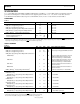
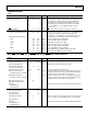
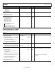
POWER DISSIPATION
Table 3.
Parameter Min Typ Max Unit Test Conditions/Comments
POWER DISSIPATION
Does not include power dissipated in termination resistors
Typical Configuration 876 970 mW Clock distribution outputs running as follows: seven LVPECL outputs
at 122.88 MHz, three LVDS outputs (3.5 mA) at 61.44 MHz, three
LVDS outputs (3.5 mA) at 245.76 MHz, one CMOS 10 pF load at
122.88 MHz, and one differential input reference at 30.72 MHz;
f
VCXO
= 122.88 MHz, f
VCO
= 3932.16 MHz; PLL2 BW = 530 kHz,
doubler is off
PD
, Power-Down 101 132.2 mW
PD
pin pulled low, with typical configuration conditions
INCREMENTAL POWER DISSIPATION
Low Power Typical Configuration 389 450 mW Absolute total power with clock distribution; one LVPECL output
running at 122.88 MHz; one differential input reference at
30.72 MHz; f
VCXO
= 122.88 MHz, f
VCO
= 3932.16 MHz; doubler is off
Output Distribution, Driver On Incremental power increase (OUT1) from low power typical
LVDS 15.3 18.4 mW Single 3.5 mA LVDS output at 245.76 MHz
47.8
55.4
mW
Single 7 mA LVDS output at 61.44 MHz
LVPECL 50.1 54.9 mW Single LVPECL output at 122.88 MHz
HSTL 40.2 46.3 mW Single 8 mA HSTL output at 122.88 MHz
43.7 50.3 mW Single 16 mA HSTL output at 122.88 MHz
CMOS 6.6 7.9 mW Single 3.3 V CMOS output at 15.36 MHz
9.9 11.9 mW Dual complementary 3.3 V CMOS output at 122.88 MHz
9.9 11.9 mW Dual in-phase 3.3 V CMOS output at 122.88 MHz
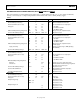
REFA,
REFA
, REFB,
REFB
, OSC_IN,
OSC_IN
, AND ZD_IN,
ZD_IN
INPUT CHARACTERISTICS
Table 4.
Parameter Min Typ Max Unit Test Conditions/Comments
DIFFERENTIAL MODE
Input Frequency Range 400 MHz
Input Slew Rate (OSC_IN)
400
V/µs
Minimum limit imposed for jitter performance
Common-Mode Internally
Generated Input Voltage
0.6
0.7
0.8
V
Input Common-Mode Range 1.025 1.475 V For dc-coupled LVDS (maximum swing)
Differential Input Voltage,
Sensitivity Frequency < 250 MHz
100 mV p-p Capacitive coupling required; can accommodate single-ended
input by ac grounding of unused input; the instantaneous voltage
on either pin must not exceed the 1.8 V dc supply rails
Differential Input Voltage,
Sensitivity Frequency > 250 MHz
200 mV p-p Capacitive coupling required; can accommodate single-ended
input by ac grounding of unused input; the instantaneous voltage
on either pin must not exceed the 1.8 V dc supply rails
Differential Input Resistance 4.8 kΩ
Differential Input Capacitance 1 pF
Duty Cycle Duty cycle bounds are set by pulse width high and pulse width low
Pulse Width Low 1 ns
Pulse Width High 1 ns
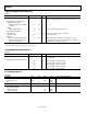
CMOS MODE SINGLE-ENDED INPUT
Input Frequency Range 250 MHz
Input High Voltage 1.62 V
Input Low Voltage 0.52 V
Input Threshold Voltage 1.0 V
When ac coupling to the input receiver, the user must dc bias the
input to 1 V; the single-ended CMOS input is 3.3 V compatible
Input Capacitance 1 pF
Duty Cycle Duty cycle bounds are set by pulse width high and pulse width low
Pulse Width Low 1.6 ns
Pulse Width High 1.6 ns