
Datasheet


AD9524 Data Sheet
Rev. D | Page 10 of 56
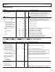
LOGIC INPUT PINS—
PD
,
SYNC
,
RESET
, EEPROM_SEL, REF_SEL
Table 13.
Parameter Min Typ Max Unit Test Conditions/Comments
VOLTAGE
Input High 2.0 V
Input Low 0.8 V
INPUT LOW CURRENT
±80
±250
µA
The minus sign indicates that, due to the
internal pull-up resistor, current is flowing
out of the AD9524
CAPACITANCE
3
pF
RESET
TIMING
Pulse Width Low 50 ns
Inactive to Start of Register Programming 100 ns
SYNC
TIMING
Pulse Width Low
1.5
ns
High speed clock is CLK input signal
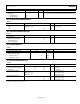
STATUS OUTPUT PINS—STATUS1, STATUS0
Table 14.
Parameter Min Typ Max Unit Test Conditions/Comments
VOLTAGE
Output High 2.94 V
Output Low 0.4 V
SERIAL CONTROL PORT—SPI MODE
Table 15.
Parameter Min Typ Max Unit Test Conditions/Comments
CS
(INPUT)
CS
has an internal 40 kΩ pull-up resistor
Voltage
Input Logic 1 2.0 V
Input Logic 0 0.8 V
Current
Input Logic 1 30 µA
Input Logic 0 −110 µA The minus sign indicates that, due to the
internal pull-up resistor, current is flowing out
of the AD9524
Input Capacitance 2 pF
SCLK (INPUT) IN SPI MODE SCLK has an internal 40 kΩ pull-down resistor
in SPI mode but not in I
2
C mode
Voltage
Input Logic 1 2.0 V
Input Logic 0 0.8 V
Current
Input Logic 1 240 µA
Input Logic 0 1 µA
Input Capacitance 2 pF
SDIO (WHEN INPUT IS IN BIDIRECTIONAL MODE)
Voltage
Input Logic 1 2.0 V
Input Logic 0 0.8 V
Current
Input Logic 1 1 µA
Input Logic 0 1 µA
Input Capacitance 2 pF