
Datasheet
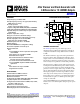


AD9524 Data Sheet
Rev. D | Page 4 of 56
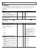
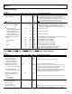
SPECIFICATIONS
f
VCXO
= 122.88 MHz single-ended, REFA and REFB on differential at 30.72 MHz, f
VCO
= 3932.16 MHz, doubler is off, channel control
low power mode off, divider phase =1, unless otherwise noted. Typical is given for VDD = 3.3 V ± 5%, and T
A
= 25°C, unless otherwise
noted. Minimum and maximum values are given over the full VDD and T
A
(−40°C to +85°C) variation, as listed in Table 1.
CONDITIONS
Table 1.
Parameter
Min
Typ
Max
Unit
Test Conditions/Comments
SUPPLY VOLTAGE
VDD3_PLL1, Supply Voltage for PLL1
3.3
V
3.3 V ± 5%
VDD3_PLL2, Supply Voltage for PLL2 3.3 V 3.3 V ± 5%
VDD3_REF, Supply Voltage Clock Output Drivers Reference 3.3 V 3.3 V ± 5%
VDD3_OUT[x:y],
1
Supply Voltage Clock Output Drivers 3.3 V 3.3 V ± 5%
VDD1.8_OUT[x:y],
1
Supply Voltage Clock Dividers 1.8 V 1.8 V ± 5%
TEMPERATURE
Ambient Temperature Range, T
A
−40 +25 +85 °C
Junction Temperature, T
J
115 °C
1
x and y are the pair of differential outputs that share the same power supply. For example, VDD3_OUT[0:1] is Supply Voltage Clock Output OUT0,
OUT0
(Pin 41 and Pin 40,
respectively) and Supply Voltage Clock Output OUT1,
OUT1
(Pin 38 and Pin 37, respectively).
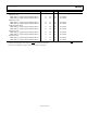
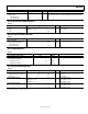
SUPPLY CURRENT
Table 2.
Parameter Min Typ Max Unit Test Conditions/Comments
SUPPLIES OTHER THAN CLOCK OUTPUT DRIVERS
VDD3_PLL1, Supply Voltage for PLL1 37 43 mA Decreases by 9 mA typical if REFB is turned
off
VDD3_PLL2, Supply Voltage for PLL2 67 77.7 mA
VDD3_REF, Supply Voltage Clock Output Drivers
Reference
LVPECL Mode
5
6
mA
Only one output driver turned on; for each
additional output that is turned on, the current
increments by 1.2 mA maximum
LVDS Mode 4 4.8 mA Only one output driver turned on; for each
additional output that is turned on, the current
increments by 1.2 mA maximum
HSTL Mode
3
3.6
mA
Values are independent of the number of
outputs turned on
CMOS Mode 3 3.6 mA Values are independent of the number of
outputs turned on
VDD1.8_OUT[x:y],
1
Supply Voltage Clock Dividers
2
3.5 4.2 mA Current for each divider: f = 245.76 MHz
CLOCK OUTPUT DRIVERS—LOWER POWER MODE OFF Channel x control register, Bit 4 = 0
LVDS Mode, 7 mA
VDD3_OUT[x:y],
1
Supply Voltage Clock Output Drivers 11.5 13.2 mA f = 122.88 MHz
VDD3_OUT[x:y],
1
Supply Voltage Clock Output Drivers
40
45
mA
f = 983.04 MHz
LVDS Mode, 3.5 mA
VDD3_OUT[x:y],
1
Supply Voltage Clock Output Drivers 6.5 7.5 mA f = 122.88 MHz
VDD3_OUT[x:y],
1
Supply Voltage Clock Output Drivers 23 26.3 mA f = 983.04 MHz
LVPECL Compatible Mode
VDD3_OUT[x:y],
1
Supply Voltage Clock Output Drivers 13 14.4 mA f = 122.88 MHz
VDD3_OUT[x:y],
1
Supply Voltage Clock Output Drivers 41 46.5 mA f = 983.04 MHz
HSTL Mode, 8 mA
VDD3_OUT[x:y],
1
Supply Voltage Clock Output Drivers 14 16.3 mA f = 122.88 MHz
CMOS Mode (Single-Ended)
VDD3_OUT[x:y],
1
Supply Voltage Clock Output Drivers 2 2.4 mA f = 15.36 MHz, 10 pF load