
Datasheet
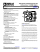


Data Sheet AD9524
Rev. D | Page 7 of 56
Parameter Min Typ Max Unit Test Conditions/Comments
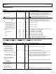
Input Capacitance 1 pF
Duty Cycle Duty cycle bounds are set by pulse width high and pulse width low
Pulse Width Low 1.6 ns
Pulse Width High 1.6 ns
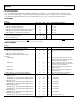
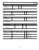
OSC_CTRL OUTPUT CHARACTERISTICS
Table 5.
Parameter Min Typ Max Unit Test Conditions/Comments
OUTPUT VOLTAGE
High VDD3_PLL1 − 0.15 V R
LOAD
> 20 kΩ
Low 150 mV
REF_TEST INPUT CHARACTERISTICS
Table 6.
Parameter Min Typ Max Unit Test Conditions/Comments
REF_TEST INPUT
Input Frequency Range 250 MHz
Input High Voltage 2.0 V
Input Low Voltage 0.8 V
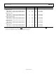
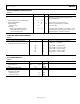
PLL1 CHARACTERISTICS
Table 7
Parameter Min Typ Max Unit Test Conditions/Comments
PLL1 FIGURE OF MERIT (FOM) −226 dBc/Hz
MAXIMUM PFD FREQUENCY
Antibacklash Pulse Width
Minimum and Low 75 MHz
Maximum and High 75 MHz
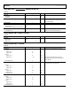
PLL1 OUTPUT CHARACTERISTICS
Table 8.
Parameter
1
Min Typ Max Unit Test Conditions/Comments
MAXIMUM OUTPUT FREQUENCY 250 MHz
Rise/Fall Time (20% to 80%) 387 665 ps 15 pF load
Duty Cycle 45 50 55 % f = 250 MHz
OUTPUT VOLTAGE HIGH Output driver static
VDD3_PLL1 − 0.25 V Load current = 10 mA
VDD3_PLL1 − 0.1 V Load current = 1 mA
OUTPUT VOLTAGE LOW Output driver static
0.2 V Load current = 10 mA
0.1 V Load current = 1 mA
1
CMOS driver strength = strong (see Table 52).